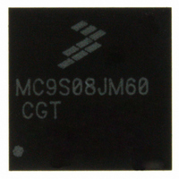
MC9S08JM60CGT Freescale Semiconductor, MC9S08JM60CGT Datasheet - Page 329

MC9S08JM60CGT
Manufacturer Part Number
MC9S08JM60CGT
Description
IC MCU 8BIT 60K FLASH 48-QFN
Manufacturer
Freescale Semiconductor
Series
HCS08r
Datasheet
1.MC9S08JM32CLD.pdf
(388 pages)
Specifications of MC9S08JM60CGT
Core Processor
HCS08
Core Size
8-Bit
Speed
48MHz
Connectivity
I²C, LIN, SCI, SPI, USB
Peripherals
LVD, POR, PWM, WDT
Number Of I /o
37
Program Memory Size
60KB (60K x 8)
Program Memory Type
FLASH
Ram Size
4K x 8
Voltage - Supply (vcc/vdd)
2.7 V ~ 5.5 V
Data Converters
A/D 8x12b
Oscillator Type
External
Operating Temperature
-40°C ~ 85°C
Package / Case
48-QFN
Processor Series
S08JM
Core
HCS08
Data Bus Width
8 bit
Data Ram Size
4 KB
Interface Type
SCI/SPI
Maximum Clock Frequency
24 MHz
Number Of Programmable I/os
37
Number Of Timers
8
Maximum Operating Temperature
+ 85 C
Mounting Style
SMD/SMT
3rd Party Development Tools
EWS08
Development Tools By Supplier
DEMOJM, DEMOJMSKT, DEMOFLEXISJMSD, DEMO9S08JM16
Minimum Operating Temperature
- 40 C
On-chip Adc
8-ch x 12-bit
Cpu Family
HCS08
Device Core Size
8b
Frequency (max)
24MHz
Total Internal Ram Size
4KB
# I/os (max)
37
Number Of Timers - General Purpose
8
Operating Supply Voltage (typ)
3.3/5V
Operating Supply Voltage (max)
5.5V
Operating Supply Voltage (min)
2.7V
Instruction Set Architecture
CISC
Operating Temp Range
-40C to 85C
Operating Temperature Classification
Industrial
Mounting
Surface Mount
Pin Count
48
Package Type
QFN EP
Package
48QFN EP
Family Name
HCS08
Maximum Speed
24 MHz
Operating Supply Voltage
3.3|5 V
For Use With
DEMOJM - KIT DEMO FOR JM MCU FAMILYDEMOJMSKT - BOARD DEMO S08JM CARD W/SOCKET
Lead Free Status / RoHS Status
Lead free / RoHS Compliant
Eeprom Size
-
Lead Free Status / Rohs Status
Lead free / RoHS Compliant
Available stocks
Company
Part Number
Manufacturer
Quantity
Price
- Current page: 329 of 388
- Download datasheet (5Mb)
Typically, a relatively simple interface pod is used to translate commands from a host computer into
commands for the custom serial interface to the single-wire background debug system. Depending on the
development tool vendor, this interface pod may use a standard RS-232 serial port, a parallel printer port,
or some other type of communications such as a universal serial bus (USB) to communicate between the
host PC and the pod. The pod typically connects to the target system with ground, the BKGD pin, RESET,
and sometimes V
which is useful to regain control of a lost target system or to control startup of a target system before the
on-chip nonvolatile memory has been programmed. Sometimes V
power from the target system to avoid the need for a separate power supply. However, if the pod is powered
separately, it can be connected to a running target system without forcing a target system reset or otherwise
disturbing the running application program.
18.2.1
BKGD is the single-wire background debug interface pin. The primary function of this pin is for
bidirectional serial communication of active background mode commands and data. During reset, this pin
is used to select between starting in active background mode or starting the user’s application program.
This pin is also used to request a timed sync response pulse to allow a host development tool to determine
the correct clock frequency for background debug serial communications.
BDC serial communications use a custom serial protocol first introduced on the M68HC12 Family of
microcontrollers. This protocol assumes the host knows the communication clock rate that is determined
by the target BDC clock rate. All communication is initiated and controlled by the host that drives a
high-to-low edge to signal the beginning of each bit time. Commands and data are sent most significant
bit first (MSB first). For a detailed description of the communications protocol, refer to
“Communication
If a host is attempting to communicate with a target MCU that has an unknown BDC clock rate, a SYNC
command may be sent to the target MCU to request a timed sync response signal from which the host can
determine the correct communication speed.
BKGD is a pseudo-open-drain pin and there is an on-chip pullup so no external pullup resistor is required.
Unlike typical open-drain pins, the external RC time constant on this pin, which is influenced by external
capacitance, plays almost no role in signal rise time. The custom protocol provides for brief, actively
driven speedup pulses to force rapid rise times on this pin without risking harmful drive level conflicts.
Refer to
Freescale Semiconductor
•
Non-intrusive commands can be executed at any time even while the user’s program is running.
Non-intrusive commands allow a user to read or write MCU memory locations or access status and
control registers within the background debug controller.
Section 18.2.2, “Communication
BKGD Pin Description
DD
Details.”
. An open-drain connection to reset allows the host to force a target system reset,
MC9S08JM60 Series Data Sheet, Rev. 3
Figure 18-1. BDM Tool Connector
NO CONNECT 3
NO CONNECT 5
Details,”
BKGD
1
for more detail.
2
4
6
GND
RESET
V
DD
DD
can be used to allow the pod to use
Development Support
Section 18.2.2,
329
Related parts for MC9S08JM60CGT
Image
Part Number
Description
Manufacturer
Datasheet
Request
R
Part Number:
Description:
Manufacturer:
Freescale Semiconductor, Inc
Datasheet:
Part Number:
Description:
Manufacturer:
Freescale Semiconductor, Inc
Datasheet:
Part Number:
Description:
Manufacturer:
Freescale Semiconductor, Inc
Datasheet:
Part Number:
Description:
Manufacturer:
Freescale Semiconductor, Inc
Datasheet:
Part Number:
Description:
Manufacturer:
Freescale Semiconductor, Inc
Datasheet:
Part Number:
Description:
Manufacturer:
Freescale Semiconductor, Inc
Datasheet:
Part Number:
Description:
Manufacturer:
Freescale Semiconductor, Inc
Datasheet:
Part Number:
Description:
Manufacturer:
Freescale Semiconductor, Inc
Datasheet:
Part Number:
Description:
Manufacturer:
Freescale Semiconductor, Inc
Datasheet:
Part Number:
Description:
Manufacturer:
Freescale Semiconductor, Inc
Datasheet:
Part Number:
Description:
Manufacturer:
Freescale Semiconductor, Inc
Datasheet:
Part Number:
Description:
Manufacturer:
Freescale Semiconductor, Inc
Datasheet:
Part Number:
Description:
Manufacturer:
Freescale Semiconductor, Inc
Datasheet:
Part Number:
Description:
Manufacturer:
Freescale Semiconductor, Inc
Datasheet:
Part Number:
Description:
Manufacturer:
Freescale Semiconductor, Inc
Datasheet:


