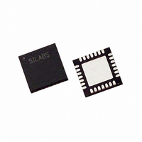
C8051F351-GM Silicon Laboratories Inc, C8051F351-GM Datasheet - Page 43

C8051F351-GM
Manufacturer Part Number
C8051F351-GM
Description
IC 8051 MCU 8K FLASH 28MLP
Manufacturer
Silicon Laboratories Inc
Series
C8051F35xr
Specifications of C8051F351-GM
Program Memory Type
FLASH
Program Memory Size
8KB (8K x 8)
Package / Case
28-MLP
Core Processor
8051
Core Size
8-Bit
Speed
50MHz
Connectivity
SMBus (2-Wire/I²C), SPI, UART/USART
Peripherals
POR, PWM, Temp Sensor, WDT
Number Of I /o
17
Ram Size
768 x 8
Voltage - Supply (vcc/vdd)
2.7 V ~ 3.6 V
Data Converters
A/D 8x24b; D/A 2x8b
Oscillator Type
Internal
Operating Temperature
-40°C ~ 85°C
Processor Series
C8051F3x
Core
8051
Data Bus Width
8 bit
Data Ram Size
768 B
Interface Type
I2C/SMBus/SPI/UART
Maximum Clock Frequency
50 MHz
Number Of Programmable I/os
17
Number Of Timers
4
Operating Supply Voltage
2.7 V to 3.6 V
Maximum Operating Temperature
+ 85 C
Mounting Style
SMD/SMT
3rd Party Development Tools
KSK-SL-TOOLSTICK, PK51, CA51, A51, ULINK2
Development Tools By Supplier
C8051F350DK
Minimum Operating Temperature
- 40 C
On-chip Adc
8-ch x 24-bit
On-chip Dac
2-ch x 8-bit
Package
28QFN
Device Core
8051
Family Name
C8051F35x
Maximum Speed
50 MHz
Data Rom Size
128 B
Height
0.88 mm
Length
5 mm
Supply Voltage (max)
3.6 V
Supply Voltage (min)
2.7 V
Width
5 mm
Lead Free Status / RoHS Status
Lead free / RoHS Compliant
For Use With
770-1006 - ISP 4PORT FOR SILABS C8051F MCU336-1083 - DEV KIT FOR F350/351/352/353
Eeprom Size
-
Lead Free Status / Rohs Status
Lead free / RoHS Compliant
Other names
336-1271
Available stocks
Company
Part Number
Manufacturer
Quantity
Price
Company:
Part Number:
C8051F351-GM
Manufacturer:
SiliconL
Quantity:
5
- Current page: 43 of 234
- Download datasheet (2Mb)
5.1.3. Modulator Clock
The ADC0CLK register (SFR Definition 5.4) holds the Modulator Clock (MDCLK) divisor value. The modu-
lator clock determines the switching frequency for the ADC sampling capacitors. Optimal performance will
be achieved when the MDCLK frequency is equal to 2.4576 MHz. The modulator samples the input at a
rate of MDCLK / 128.
5.1.4. Decimation Ratio
The decimation ratio of the ADC filters is selected by the DECI[10:0] bits in the ADC0DECH and
ADC0DECL registers (SFR Definition 5.5 and SFR Definition 5.6, respectively). The decimation ratio is
equal to 1 + DECI[10:0]. The decimation ratio determines how many modulator samples are used to gen-
erate a single output word. The ADC output word rate is equal to the modulator sampling rate divided by
the decimation ratio. For more information on how the ADC output word rate is derived, see SFR Definition
5.4 and SFR Definition 5.6. Higher decimation ratios will produce lower-noise results over a longer conver-
sion period. The minimum decimation ratio is 20. When using the fast filter output, the decimation ratio
must be set to a multiple of 8.
Channel
Channel
AIN+
AIN-
Figure 5.2. ADC0 Buffer Control
Bypass Buffer
Bypass Buffer
High Buffer+
Low Buffer+
High Buffer-
Low Buffer-
Rev. 1.1
AD0BPHE
AD0BNHE
AD0BNLE
AD0BNS1
AD0BNS0
AD0BPLE
AD0BPS1
AD0BPS0
To PGA
To PGA
C8051F350/1/2/3
43
Related parts for C8051F351-GM
Image
Part Number
Description
Manufacturer
Datasheet
Request
R
Part Number:
Description:
SMD/C°/SINGLE-ENDED OUTPUT SILICON OSCILLATOR
Manufacturer:
Silicon Laboratories Inc
Part Number:
Description:
Manufacturer:
Silicon Laboratories Inc
Datasheet:
Part Number:
Description:
N/A N/A/SI4010 AES KEYFOB DEMO WITH LCD RX
Manufacturer:
Silicon Laboratories Inc
Datasheet:
Part Number:
Description:
N/A N/A/SI4010 SIMPLIFIED KEY FOB DEMO WITH LED RX
Manufacturer:
Silicon Laboratories Inc
Datasheet:
Part Number:
Description:
N/A/-40 TO 85 OC/EZLINK MODULE; F930/4432 HIGH BAND (REV E/B1)
Manufacturer:
Silicon Laboratories Inc
Part Number:
Description:
EZLink Module; F930/4432 Low Band (rev e/B1)
Manufacturer:
Silicon Laboratories Inc
Part Number:
Description:
I°/4460 10 DBM RADIO TEST CARD 434 MHZ
Manufacturer:
Silicon Laboratories Inc
Part Number:
Description:
I°/4461 14 DBM RADIO TEST CARD 868 MHZ
Manufacturer:
Silicon Laboratories Inc
Part Number:
Description:
I°/4463 20 DBM RFSWITCH RADIO TEST CARD 460 MHZ
Manufacturer:
Silicon Laboratories Inc
Part Number:
Description:
I°/4463 20 DBM RADIO TEST CARD 868 MHZ
Manufacturer:
Silicon Laboratories Inc
Part Number:
Description:
I°/4463 27 DBM RADIO TEST CARD 868 MHZ
Manufacturer:
Silicon Laboratories Inc
Part Number:
Description:
I°/4463 SKYWORKS 30 DBM RADIO TEST CARD 915 MHZ
Manufacturer:
Silicon Laboratories Inc
Part Number:
Description:
N/A N/A/-40 TO 85 OC/4463 RFMD 30 DBM RADIO TEST CARD 915 MHZ
Manufacturer:
Silicon Laboratories Inc
Part Number:
Description:
I°/4463 20 DBM RADIO TEST CARD 169 MHZ
Manufacturer:
Silicon Laboratories Inc


