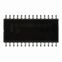
MC908QC16CDZE Freescale Semiconductor, MC908QC16CDZE Datasheet - Page 203

MC908QC16CDZE
Manufacturer Part Number
MC908QC16CDZE
Description
IC MCU 8BIT 16K FLASH 28-SOIC
Manufacturer
Freescale Semiconductor
Series
HC08r
Specifications of MC908QC16CDZE
Core Processor
HC08
Core Size
8-Bit
Speed
8MHz
Connectivity
SCI, SPI
Peripherals
LVD, POR, PWM
Number Of I /o
24
Program Memory Size
16KB (16K x 8)
Program Memory Type
FLASH
Ram Size
512 x 8
Voltage - Supply (vcc/vdd)
3 V ~ 5.5 V
Data Converters
A/D 10x10b
Oscillator Type
Internal
Operating Temperature
-40°C ~ 85°C
Package / Case
28-SOIC (7.5mm Width)
Processor Series
HC08QC
Core
HC08
Data Bus Width
8 bit
Data Ram Size
512 B
Interface Type
ESCI/SPI
Maximum Clock Frequency
8 MHz
Number Of Programmable I/os
26
Number Of Timers
6
Maximum Operating Temperature
+ 85 C
Mounting Style
SMD/SMT
Development Tools By Supplier
FSICEBASE, M68CBL05AE, DEMO908QB8, DEMO908QC16
Minimum Operating Temperature
- 40 C
On-chip Adc
10-ch x 10-bit
For Use With
DEMO908QC16 - BOARD DEMO FOR MC908QC16
Lead Free Status / RoHS Status
Lead free / RoHS Compliant
Eeprom Size
-
Lead Free Status / Rohs Status
Lead free / RoHS Compliant
Available stocks
Company
Part Number
Manufacturer
Quantity
Price
Company:
Part Number:
MC908QC16CDZE
Manufacturer:
FREESCALE
Quantity:
1 600
Part Number:
MC908QC16CDZE
Manufacturer:
FREESCALE
Quantity:
20 000
- Current page: 203 of 274
- Download datasheet (4Mb)
TOVx — Toggle-On-Overflow Bit
CHxMAX — Channel x Maximum Duty Cycle Bit
Freescale Semiconductor
When ELSxB and ELSxA are both clear, channel x is not connected to an I/O port, and pin T1CHx is
available as a general-purpose I/O pin.
When channel x is an output compare channel, this read/write bit controls the behavior of the channel
x output when the counter overflows. When channel x is an input capture channel, TOVx has no effect.
When the TOVx bit is at 1, setting the CHxMAX bit forces the duty cycle of buffered and unbuffered
PWM signals to 100%. As
or cleared. The output stays at the 100% duty cycle level until the cycle after CHxMAX is cleared.
1 = Channel x pin toggles on counter overflow.
0 = Channel x pin does not toggle on counter overflow.
After initially enabling a TIM1 channel register for input capture operation
and selecting the edge sensitivity, clear CHxF to ignore any erroneous
edge detection flags.
When TOVx is set, a counter overflow takes precedence over a channel x
output compare if both occur at the same time.
CHxMAX
T1CHx
MC68HC908QC16 • MC68HC908QC8 • MC68HC908QC4 Data Sheet, Rev. 5
OVERFLOW
Figure 16-13
COMPARE
PERIOD
OUTPUT
Figure 16-13. CHxMAX Latency
OVERFLOW
Table 16-2
shows, the CHxMAX bit takes effect in the cycle after it is set
COMPARE
OUTPUT
NOTE
NOTE
OVERFLOW
shows how ELSxB and ELSxA work.
COMPARE
OUTPUT
OVERFLOW
COMPARE
OUTPUT
OVERFLOW
Registers
203
Related parts for MC908QC16CDZE
Image
Part Number
Description
Manufacturer
Datasheet
Request
R
Part Number:
Description:
Manufacturer:
Freescale Semiconductor, Inc
Datasheet:
Part Number:
Description:
Manufacturer:
Freescale Semiconductor, Inc
Datasheet:
Part Number:
Description:
Manufacturer:
Freescale Semiconductor, Inc
Datasheet:
Part Number:
Description:
Manufacturer:
Freescale Semiconductor, Inc
Datasheet:
Part Number:
Description:
Manufacturer:
Freescale Semiconductor, Inc
Datasheet:
Part Number:
Description:
Manufacturer:
Freescale Semiconductor, Inc
Datasheet:
Part Number:
Description:
Manufacturer:
Freescale Semiconductor, Inc
Datasheet:
Part Number:
Description:
Manufacturer:
Freescale Semiconductor, Inc
Datasheet:
Part Number:
Description:
Manufacturer:
Freescale Semiconductor, Inc
Datasheet:
Part Number:
Description:
Manufacturer:
Freescale Semiconductor, Inc
Datasheet:
Part Number:
Description:
Manufacturer:
Freescale Semiconductor, Inc
Datasheet:
Part Number:
Description:
Manufacturer:
Freescale Semiconductor, Inc
Datasheet:
Part Number:
Description:
Manufacturer:
Freescale Semiconductor, Inc
Datasheet:
Part Number:
Description:
Manufacturer:
Freescale Semiconductor, Inc
Datasheet:
Part Number:
Description:
Manufacturer:
Freescale Semiconductor, Inc
Datasheet:


