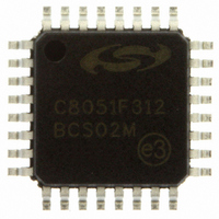
C8051F312-GQ Silicon Laboratories Inc, C8051F312-GQ Datasheet - Page 108

C8051F312-GQ
Manufacturer Part Number
C8051F312-GQ
Description
IC 8051 MCU 8K FLASH 32LQFP
Manufacturer
Silicon Laboratories Inc
Series
C8051F31xr
Specifications of C8051F312-GQ
Program Memory Type
FLASH
Program Memory Size
8KB (8K x 8)
Package / Case
32-LQFP
Core Processor
8051
Core Size
8-Bit
Speed
25MHz
Connectivity
SMBus (2-Wire/I²C), SPI, UART/USART
Peripherals
POR, PWM, Temp Sensor, WDT
Number Of I /o
29
Ram Size
1.25K x 8
Voltage - Supply (vcc/vdd)
2.7 V ~ 3.6 V
Data Converters
A/D 21x10b
Oscillator Type
Internal
Operating Temperature
-40°C ~ 85°C
Processor Series
C8051F3x
Core
8051
Data Bus Width
8 bit
Data Ram Size
1.25 KB
Interface Type
I2C, SMBus, SPI, UART
Maximum Clock Frequency
25 MHz
Number Of Programmable I/os
29
Number Of Timers
4 bit
Operating Supply Voltage
2.7 V to 3.6 V
Maximum Operating Temperature
+ 85 C
Mounting Style
SMD/SMT
3rd Party Development Tools
PK51, CA51, A51, ULINK2
Development Tools By Supplier
C8051F310DK
Minimum Operating Temperature
- 40 C
On-chip Adc
10 bit, 21 Channel
No. Of I/o's
29
Ram Memory Size
1280Byte
Cpu Speed
25MHz
No. Of Timers
4
Rohs Compliant
Yes
Package
32LQFP
Device Core
8051
Family Name
C8051F31x
Maximum Speed
25 MHz
Lead Free Status / RoHS Status
Lead free / RoHS Compliant
For Use With
336-1445 - ADAPTER PROGRAM TOOLSTICK F310
Eeprom Size
-
Lead Free Status / Rohs Status
Lead free / RoHS Compliant
Other names
336-1255
Available stocks
Company
Part Number
Manufacturer
Quantity
Price
Company:
Part Number:
C8051F312-GQ
Manufacturer:
Silicon Laboratories Inc
Quantity:
10 000
Company:
Part Number:
C8051F312-GQR
Manufacturer:
Silicon Laboratories Inc
Quantity:
10 000
C8051F310/1/2/3/4/5/6/7
9.4.
The Missing Clock Detector (MCD) is a one-shot circuit that is triggered by the system clock. If the system
clock remains high or low for more than 100 µs, the one-shot will time out and generate a reset. After a
MCD reset, the MCDRSF flag (RSTSRC.2) will read ‘1’, signifying the MCD as the reset source; otherwise,
this bit reads ‘0’. Writing a ‘1’ to the MCDRSF bit enables the Missing Clock Detector; writing a ‘0’ disables
it. The state of the RST pin is unaffected by this reset.
9.5.
Comparator0 can be configured as a reset source by writing a ‘1’ to the C0RSEF flag (RSTSRC.5).
Comparator0 should be enabled and allowed to settle prior to writing to C0RSEF to prevent any turn-on
chatter on the output from generating an unwanted reset. The Comparator0 reset is active-low: if the non-
inverting input voltage (on CP0+) is less than the inverting input voltage (on CP0-), the device is put into
the reset state. After a Comparator0 reset, the C0RSEF flag (RSTSRC.5) will read ‘1’ signifying
Comparator0 as the reset source; otherwise, this bit reads ‘0’. The state of the RST pin is unaffected by
this reset.
9.6.
The programmable Watchdog Timer (WDT) function of the Programmable Counter Array (PCA) can be
used to prevent software from running out of control during a system malfunction. The PCA WDT function
can be enabled or disabled by software as described in
page
prevents user software from updating the WDT, a reset is generated and the WDTRSF bit (RSTSRC.5) is
set to ‘1’. The state of the RST pin is unaffected by this reset.
9.7.
If a Flash read/write/erase or program read targets an illegal address, a system reset is generated. This
may occur due to any of the following:
•
•
•
•
The FERROR bit (RSTSRC.6) is set following a Flash error reset. The state of the RST pin is unaffected by
this reset.
9.8.
Software may force a reset by writing a ‘1’ to the SWRSF bit (RSTSRC.4). The SWRSF bit will read ‘1’ fol-
lowing a software forced reset. The state of the RST pin is unaffected by this reset.
108
A Flash write or erase is attempted above user code space. This occurs when PSWE is set to ‘1’ and a
MOVX write operation targets an address above address 0x3DFF for C8051F310/1 or 0x1FFF for
C8051F312/3/4/5.
A Flash read is attempted above user code space. This occurs when a MOVC operation targets an
address above address 0x3DFF for C8051F310/1 or 0x1FFF for C8051F312/3/4/5.
A Program read is attempted above user code space. This occurs when user code attempts to branch
to an address above 0x3DFF for C8051F310/1 or 0x1FFF for C8051F312/3/4/5.
A Flash read, write or erase attempt is restricted due to a Flash security setting (see
“10.3. Security Options” on page
212; the WDT is enabled and clocked by SYSCLK / 12 following any reset. If a system malfunction
Missing Clock Detector Reset
Comparator0 Reset
PCA Watchdog Timer Reset
Flash Error Reset
Software Reset
113).
Rev. 1.7
Section “18.3. Watchdog Timer Mode” on
Section


