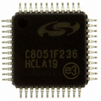
C8051F236-GQ Silicon Laboratories Inc, C8051F236-GQ Datasheet - Page 59

C8051F236-GQ
Manufacturer Part Number
C8051F236-GQ
Description
IC 8051 MCU 8K FLASH 48TQFP
Manufacturer
Silicon Laboratories Inc
Series
C8051F2xxr
Specifications of C8051F236-GQ
Program Memory Type
FLASH
Program Memory Size
8KB (8K x 8)
Package / Case
48-TQFP, 48-VQFP
Core Processor
8051
Core Size
8-Bit
Speed
25MHz
Connectivity
SPI, UART/USART
Peripherals
Brown-out Detect/Reset, POR, WDT
Number Of I /o
32
Ram Size
1.25K x 8
Voltage - Supply (vcc/vdd)
2.7 V ~ 3.6 V
Oscillator Type
Internal
Operating Temperature
-40°C ~ 85°C
Processor Series
C8051F2x
Core
8051
Data Bus Width
8 bit
Data Ram Size
1.25 KB
Interface Type
SPI/UART
Maximum Clock Frequency
25 MHz
Number Of Programmable I/os
32
Number Of Timers
3
Operating Supply Voltage
2.7 V to 3.6 V
Maximum Operating Temperature
+ 85 C
Mounting Style
SMD/SMT
3rd Party Development Tools
PK51, CA51, A51, ULINK2
Development Tools By Supplier
C8051F226DK
Minimum Operating Temperature
- 40 C
On-chip Adc
8 bit, 32 Channel
Lead Free Status / RoHS Status
Lead free / RoHS Compliant
Eeprom Size
-
Data Converters
-
Lead Free Status / Rohs Status
Lead free / RoHS Compliant
Other names
336-1244
Available stocks
Company
Part Number
Manufacturer
Quantity
Price
Company:
Part Number:
C8051F236-GQ
Manufacturer:
Silicon Laboratories Inc
Quantity:
10 000
Company:
Part Number:
C8051F236-GQR
Manufacturer:
MICROCHIP
Quantity:
2 500
Company:
Part Number:
C8051F236-GQR
Manufacturer:
Silicon Laboratories Inc
Quantity:
10 000
Performance
The CIP-51 employs a pipelined architecture that greatly increases its instruction throughput over the stan-
dard 8051 architecture. In a standard 8051, all instructions except for MUL and DIV take 12 or 24 system
clock cycles to execute, and usually have a maximum system clock of 12MHz. By contrast, the CIP-51
core executes 70% of its instructions in one or two system clock cycles, with no instructions taking more
than eight system clock cycles.
With the CIP-51’s maximum system clock at 25MHz, it has a peak throughput of 25MIPS. The CIP-51 has
a total of 109 instructions. The number of instructions versus the system clock cycles required to execute
them is as follows:
Programming and Debugging Support
A JTAG-based serial interface is provided for in-system programming of the Flash program memory and
communication with on-chip debug support logic. The re-programmable Flash can also be read and
changed a single byte at a time by the application software using the MOVC and MOVX instructions. This
feature allows program memory to be used for non-volatile data storage as well as updating program code
under software control.
The on-chip debug support circuitry facilitates full speed in-circuit debugging, allowing the setting of hard-
ware breakpoints and watchpoints, starting, stopping and single stepping through program execution
(including interrupt service routines), examination of the program’s call stack, and reading/writing the con-
tents of registers and memory. This method of on-chip debugging is completely non-intrusive and non-
invasive, requiring no RAM, Stack, timers, or other on-chip resources.
The CIP-51 is supported by development tools from Silicon Laboratories and third party vendors. Silicon
Labs provides an integrated development environment (IDE) including editor, macro assembler, debugger
and programmer. The IDE’s debugger and programmer interface to the CIP-51 via its JTAG interface to
provide fast and efficient in-system device programming and debugging. Third party macro assemblers
and C compilers are also available.
Clocks to Execute
Instructions
26
1
50
2
2/3
5
Rev. 1.6
14
3
3/4
7
3
4
C8051F2xx
4/5
1
2
5
1
8
59


