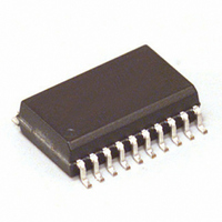
MCR908JK3ECDWE Freescale Semiconductor, MCR908JK3ECDWE Datasheet - Page 85

MCR908JK3ECDWE
Manufacturer Part Number
MCR908JK3ECDWE
Description
IC MCU 4K FLASH 8MHZ 20-SOIC
Manufacturer
Freescale Semiconductor
Series
HC08r
Datasheet
1.MC908JK1ECDWE.pdf
(180 pages)
Specifications of MCR908JK3ECDWE
Core Processor
HC08
Core Size
8-Bit
Speed
8MHz
Peripherals
LED, LVD, POR, PWM
Number Of I /o
15
Program Memory Size
4KB (4K x 8)
Program Memory Type
FLASH
Ram Size
128 x 8
Voltage - Supply (vcc/vdd)
2.7 V ~ 3.3 V
Data Converters
A/D 12x8b
Oscillator Type
External
Operating Temperature
-40°C ~ 85°C
Package / Case
20-SOIC (7.5mm Width)
Processor Series
HC08JK
Core
HC08
Data Bus Width
8 bit
Data Ram Size
128 B
Maximum Clock Frequency
8 MHz
Number Of Programmable I/os
15
Number Of Timers
2
Maximum Operating Temperature
+ 85 C
Mounting Style
SMD/SMT
Development Tools By Supplier
FSICEBASE, DEMO908JL16E, M68CBL05CE
Minimum Operating Temperature
- 40 C
On-chip Adc
8 bit, 12 Channel
Lead Free Status / RoHS Status
Lead free / RoHS Compliant
Eeprom Size
-
Connectivity
-
Lead Free Status / Rohs Status
Details
Available stocks
Company
Part Number
Manufacturer
Quantity
Price
Part Number:
MCR908JK3ECDWE
Manufacturer:
FREESCALE
Quantity:
20 000
control the output are the ones written to last. TSC0 controls and monitors the buffered output compare
function, and TIM channel 1 status and control register (TSC1) is unused. While the MS0B bit is set, the
channel 1 pin, TCH1, is available as a general-purpose I/O pin.
8.4.4 Pulse Width Modulation (PWM)
By using the toggle-on-overflow feature with an output compare channel, the TIM can generate a PWM
signal. The value in the TIM counter modulo registers determines the period of the PWM signal. The
channel pin toggles when the counter reaches the value in the TIM counter modulo registers. The time
between overflows is the period of the PWM signal.
As
of the PWM signal. The time between overflow and output compare is the pulse width. Program the TIM
to clear the channel pin on output compare if the state of the PWM pulse is logic one. Program the TIM
to set the pin if the state of the PWM pulse is logic zero.
The value in the TIM counter modulo registers and the selected prescaler output determines the
frequency of the PWM output. The frequency of an 8-bit PWM signal is variable in 256 increments. Writing
$00FF (255) to the TIM counter modulo registers produces a PWM period of 256 times the internal bus
clock period if the prescaler select value is 000 (see
The value in the TIM channel registers determines the pulse width of the PWM output. The pulse width of
an 8-bit PWM signal is variable in 256 increments. Writing $0080 (128) to the TIM channel registers
produces a duty cycle of 128/256 or 50%.
Freescale Semiconductor
Figure 8-3
shows, the output compare value in the TIM channel registers determines the pulse width
In buffered output compare operation, do not write new output compare
values to the currently active channel registers. User software should track
the currently active channel to prevent writing a new value to the active
channel. Writing to the active channel registers is the same as generating
unbuffered output compares.
TCHx
OVERFLOW
Figure 8-3. PWM Period and Pulse Width
PULSE
WIDTH
MC68HC908JL3E Family Data Sheet, Rev. 4
PERIOD
COMPARE
OUTPUT
OVERFLOW
NOTE
8.9.1 TIM Status and Control Register
COMPARE
OUTPUT
OVERFLOW
COMPARE
OUTPUT
Functional Description
(TSC)).
85


