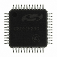
C8051F230-GQ Silicon Laboratories Inc, C8051F230-GQ Datasheet

C8051F230-GQ
Manufacturer Part Number
C8051F230-GQ
Description
IC 8051 MCU 8K FLASH 48TQFP
Manufacturer
Silicon Laboratories Inc
Series
C8051F2xxr
Specifications of C8051F230-GQ
Program Memory Type
FLASH
Program Memory Size
8KB (8K x 8)
Package / Case
48-TQFP, 48-VQFP
Core Processor
8051
Core Size
8-Bit
Speed
25MHz
Connectivity
SPI, UART/USART
Peripherals
Brown-out Detect/Reset, POR, WDT
Number Of I /o
32
Ram Size
256 x 8
Voltage - Supply (vcc/vdd)
2.7 V ~ 3.6 V
Oscillator Type
Internal
Operating Temperature
-40°C ~ 85°C
Processor Series
C8051F2x
Core
8051
Data Bus Width
8 bit
Data Ram Size
256 B
Interface Type
SPI/UART
Maximum Clock Frequency
25 MHz
Number Of Programmable I/os
32
Number Of Timers
3
Operating Supply Voltage
2.7 V to 3.6 V
Maximum Operating Temperature
+ 85 C
Mounting Style
SMD/SMT
3rd Party Development Tools
PK51, CA51, A51, ULINK2
Development Tools By Supplier
C8051F226DK
Minimum Operating Temperature
- 40 C
No. Of I/o's
32
Ram Memory Size
256Byte
Cpu Speed
25MHz
No. Of Timers
3
Rohs Compliant
Yes
Package
48TQFP
Device Core
8051
Family Name
C8051F2xx
Maximum Speed
25 MHz
Lead Free Status / RoHS Status
Lead free / RoHS Compliant
Eeprom Size
-
Data Converters
-
Lead Free Status / Rohs Status
Lead free / RoHS Compliant
Other names
336-1242
Available stocks
Company
Part Number
Manufacturer
Quantity
Price
Company:
Part Number:
C8051F230-GQ
Manufacturer:
SiliconL
Quantity:
138
Company:
Part Number:
C8051F230-GQ
Manufacturer:
Silicon Laboratories Inc
Quantity:
10 000
Company:
Part Number:
C8051F230-GQR
Manufacturer:
Silicon Laboratories Inc
Quantity:
10 000
Analog Peripherals
Two comparators
-
-
V
On-Chip JTAG Debug
-
-
-
-
Supply Voltage: 2.7 to 3.6 V
-
-
General Purpose
DD
MONEN
XTAL1
XTAL2
Programmable hysteresis
Configurable to generate interrupts or reset
On-chip emulation circuitry facilitates full-speed, non-intrusive, in-circuit
emulation
Supports breakpoints, single stepping, watchpoints, inspect/modify
memory, and registers
Superior performance to emulation systems using ICE-chips, target
pods, and sockets
Fully compliant with IEEE 1149.1 specification
Typical operating current: 9 mA at 25 MHz
Typical stop mode current: <0.1 uA
GND
GND
VDD
VDD
TMS
TDO
TCK
RST
Monitor and Brown-out Detector
TDI
NC
NC
NC
NC
Analog/Digital
Power
Oscillator
Oscillator
External
Monitor
Internal
Circuit
JTAG
Logic
VDD
Debug HW
WDT
System Clock
Reset
Copyright © 2004 by Silicon Laboratories
C
o
8
0
5
1
e
r
SFR Bus
8 kB FLASH
256 byte
25 MIPS, 8 kB Flash, 48-Pin Mixed-Signal MCU
RAM
High-Speed 8051 µC Core
-
-
-
Memory
-
-
Digital Peripherals
-
-
-
-
Clock Sources
-
-
-
48-Pin TQFP
-
Pipelined instruction architecture; executes 70% of instructions in 1 or 2
system clocks
Up to 25 MIPS throughput with 25 MHz system clock
Expanded interrupt handler; up to 21 interrupt sources
256 bytes data RAM
8 kB Flash; in-system programmable in 512 byte sectors (512 bytes are
reserved)
32 port I/O; all are 5 V tolerant
Hardware SPI™ and UART serial ports available concurrently
3 general-purpose 16-bit counter/timers
Dedicated watchdog timer; bidirectional reset
Internal programmable oscillator: 2–16 MHz
External oscillator: Crystal, RC, C, or Clock
Can switch between clock sources on-the-fly
Temperature Range: –40 to +85 °C
CP0
CP1
Timer 0
Timer 1
Timer 2
Port 0
UART
Port 1
Port 2
Port 3
Latch
Latch
Latch
Latch
SPI
CP0
CP1
CP0+
CP0-
CP1+
CP1-
SYSCLK
M
M
M
P
U
X
P
U
X
P
U
X
0
1
2
C8051F230
P
D
P
D
P
D
P
D
0
v
1
v
2
v
3
v
r
r
r
r
P0.0/TX
P0.1/RX
P0.2//INT0
P0.3//INT1
P0.4/T0
P0.5/T1
P0.6/T2
P0.7/T2EX
P1.0/CP0+
P1.1/CP0-
P1.2/CP0
P1.3/CP1+
P1.4/CP1-
P1.5/CP1
P1.6/SYSCLK
P1.7
P2.0/SCK
P2.1/MISO
P2.2/MOSI
P2.3/NSS
P2.4
P2.5
P2.6
P2.7
P3.0
P3.1
P3.2
P3.3
P3.4
P3.5
P3.6
P3.7
6.15.2004
Related parts for C8051F230-GQ
C8051F230-GQ Summary of contents
Page 1
... Latch UART Timer 0 Timer 1 Timer 2 Port 1 Latch FLASH 0 CP0 256 byte 5 RAM 1 CP1 C Port 2 o SFR Bus Latch r SPI e Port 3 Latch Copyright © 2004 by Silicon Laboratories C8051F230 P0.0/TX P P0.1/ P0.2//INT0 0 P0.3//INT1 D P0.4/T0 P0.5/ P0.6/ P0.7/T2EX X P1.0/CP0+ P P1.1/CP0 P1.2/CP0 1 CP0+ P1 ...
Page 2
... Monitor DD Monitor DD DC C8051F226DK Development Kit MIN NOM MAX (mm) (mm) (mm 1.20 A1 0.05 - 0.15 A2 0.95 1.00 1.05 b 0.17 0. 7.00 - Copyright © 2004 by Silicon Laboratories C8051F230 TYP MAX UNITS 3 0 µA 10 µA 0.1 µA 25 MHz 1.5 µA 4.0 µs 6.15.2004 ...


