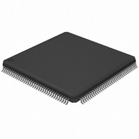
AT32UC3A0128-ALUT Atmel, AT32UC3A0128-ALUT Datasheet - Page 119

AT32UC3A0128-ALUT
Manufacturer Part Number
AT32UC3A0128-ALUT
Description
IC MCU AVR32 128KB FLASH 144LQFP
Manufacturer
Atmel
Series
AVR®32 UC3r
Specifications of AT32UC3A0128-ALUT
Core Processor
AVR
Core Size
32-Bit
Speed
66MHz
Connectivity
EBI/EMI, Ethernet, I²C, SPI, SSC, UART/USART, USB OTG
Peripherals
Brown-out Detect/Reset, POR, PWM, WDT
Number Of I /o
109
Program Memory Size
128KB (128K x 8)
Program Memory Type
FLASH
Ram Size
32K x 8
Voltage - Supply (vcc/vdd)
1.65 V ~ 1.95 V
Data Converters
A/D 8x10b
Oscillator Type
Internal
Operating Temperature
-40°C ~ 85°C
Package / Case
144-LQFP
Processor Series
AT32UC3x
Core
AVR32
Data Bus Width
32 bit
Data Ram Size
32 KB
Interface Type
2-Wire, RS-485, SPI, USART
Maximum Clock Frequency
66 MHz
Number Of Programmable I/os
69
Number Of Timers
3
Maximum Operating Temperature
+ 85 C
Mounting Style
SMD/SMT
3rd Party Development Tools
EWAVR32, EWAVR32-BL, KSK-EVK1100-PL
Development Tools By Supplier
ATAVRDRAGON, ATSTK500, ATSTK600, ATAVRISP2, ATAVRONEKIT, ATEXTWIFI, ATEVK1100, ATEVK1105
Minimum Operating Temperature
- 40 C
Controller Family/series
AT32UC3A
No. Of I/o's
109
Ram Memory Size
32KB
Cpu Speed
66MHz
No. Of Timers
1
Rohs Compliant
Yes
For Use With
ATEVK1105 - KIT EVAL FOR AT32UC3A0ATAVRONEKIT - KIT AVR/AVR32 DEBUGGER/PROGRMMR770-1008 - ISP 4PORT ATMEL AVR32 MCU SPIATEVK1100 - KIT DEV/EVAL FOR AVR32 AT32UC3A
Lead Free Status / RoHS Status
Lead free / RoHS Compliant
Eeprom Size
-
Lead Free Status / Rohs Status
Lead free / RoHS Compliant
Available stocks
Company
Part Number
Manufacturer
Quantity
Price
Company:
Part Number:
AT32UC3A0128-ALUT
Manufacturer:
Atmel
Quantity:
166
- Current page: 119 of 826
- Download datasheet (20Mb)
18.5.1
32058J–AVR32–04/11
Write/erase page operation
letting the CPU enter sleep mode after writing to FCMD, or by polling FSR for command com-
pletion. This polling will result in an access pattern with IDLE HSB cycles.
All the commands are protected by the same keyword, which has to be written in the eight
highest bits of the FCMD register. Writing FCMD with data that does not contain the correct
key and/or with an invalid command has no effect on the flash memory; however, the PROGE
flag is set in the Flash Status Register (FSR). This flag is automatically cleared by a read
access to the FSR register.
Writing a command to FCMD while another command is being executed has no effect on the
flash memory; however, the PROGE flag is set in the Flash Status Register (FSR). This flag is
automatically cleared by a read access to the FSR register.
If the current command writes or erases a page in a locked region, or a page protected by the
BOOTPROT fuses, the command has no effect on the flash memory; however, the LOCKE
flag is set in the FSR register. This flag is automatically cleared by a read access to the FSR
register.
Flash technology requires that an erase must be done before programming. The entire flash
can be erased by an Erase All command. Alternatively, pages can be individually erased by
the Erase Page command.
The User page can be written and erased using the mechanisms described in this chapter.
After programming, the page can be locked to prevent miscellaneous write or erase
sequences. Locking is performed on a per-region basis, so locking a region locks all pages
inside the region. Additional protection is provided for the lowermost address space of the
flash. This address space is allocated for the Boot Loader, and is protected both by the lock
bit(s) corresponding to this address space, and the BOOTPROT[2:0] fuses.
Data to be written are stored in an internal buffer called page buffer. The page buffer contains
w words. The page buffer wraps around within the internal memory area address space and
appears to be repeated by the number of pages in it. Writing of 8-bit and 16-bit data to the
page buffer is not allowed and may lead to unpredictable data corruption.
Data must be written to the page buffer before the programming command is written to the
Flash Command Register FCMD. The sequence is as follows:
Two errors can be detected in the FSR register after a programming sequence:
• Reset the page buffer with the Clear Page Buffer command.
• Fill the page buffer with the desired contents, using only 32-bit access.
• Programming starts as soon as the programming key and the programming command are
• When programming is completed, the bit FRDY in the Flash Status Register (FSR) is set. If
• Programming Error: A bad keyword and/or an invalid command have been written in the
written to the Flash Command Register. The PAGEN field in the Flash Command Register
(FCMD) must contain the address of the page to write. PAGEN is automatically updated
when writing to the page buffer, but can also be written to directly. The FRDY bit in the
Flash Status Register (FSR) is automatically cleared when the page write operation starts.
an interrupt was enabled by setting the bit FRDY in FCR, the interrupt line of the flash
controller is set.
FCMD register.
AT32UC3A
119
Related parts for AT32UC3A0128-ALUT
Image
Part Number
Description
Manufacturer
Datasheet
Request
R

Part Number:
Description:
DEV KIT FOR AVR/AVR32
Manufacturer:
Atmel
Datasheet:

Part Number:
Description:
INTERVAL AND WIPE/WASH WIPER CONTROL IC WITH DELAY
Manufacturer:
ATMEL Corporation
Datasheet:

Part Number:
Description:
Low-Voltage Voice-Switched IC for Hands-Free Operation
Manufacturer:
ATMEL Corporation
Datasheet:

Part Number:
Description:
MONOLITHIC INTEGRATED FEATUREPHONE CIRCUIT
Manufacturer:
ATMEL Corporation
Datasheet:

Part Number:
Description:
AM-FM Receiver IC U4255BM-M
Manufacturer:
ATMEL Corporation
Datasheet:

Part Number:
Description:
Monolithic Integrated Feature Phone Circuit
Manufacturer:
ATMEL Corporation
Datasheet:

Part Number:
Description:
Multistandard Video-IF and Quasi Parallel Sound Processing
Manufacturer:
ATMEL Corporation
Datasheet:

Part Number:
Description:
High-performance EE PLD
Manufacturer:
ATMEL Corporation
Datasheet:

Part Number:
Description:
8-bit Flash Microcontroller
Manufacturer:
ATMEL Corporation
Datasheet:

Part Number:
Description:
2-Wire Serial EEPROM
Manufacturer:
ATMEL Corporation
Datasheet:


