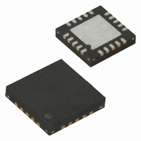
ATTINY84-20MU Atmel, ATTINY84-20MU Datasheet - Page 124

ATTINY84-20MU
Manufacturer Part Number
ATTINY84-20MU
Description
IC MCU AVR 8K FLASH 20MHZ 20-QFN
Manufacturer
Atmel
Series
AVR® ATtinyr
Specifications of ATTINY84-20MU
Core Processor
AVR
Core Size
8-Bit
Speed
20MHz
Connectivity
USI
Peripherals
Brown-out Detect/Reset, POR, PWM, Temp Sensor, WDT
Number Of I /o
12
Program Memory Size
8KB (4K x 16)
Program Memory Type
FLASH
Eeprom Size
512 x 8
Ram Size
512 x 8
Voltage - Supply (vcc/vdd)
2.7 V ~ 5.5 V
Data Converters
A/D 8x10b
Oscillator Type
Internal
Operating Temperature
-40°C ~ 85°C
Package / Case
20-MLF®, QFN
Cpu Family
ATtiny
Device Core
AVR
Device Core Size
8b
Frequency (max)
20MHz
Interface Type
SPI/USI
Total Internal Ram Size
512Byte
# I/os (max)
12
Number Of Timers - General Purpose
2
Operating Supply Voltage (typ)
3.3/5V
Operating Supply Voltage (max)
5.5V
Operating Supply Voltage (min)
2.7V
On-chip Adc
8-chx10-bit
Instruction Set Architecture
RISC
Operating Temp Range
-40C to 85C
Operating Temperature Classification
Industrial
Mounting
Surface Mount
Pin Count
20
Package Type
MLF
Processor Series
ATTINY8x
Core
AVR8
Data Bus Width
8 bit
Data Ram Size
512 B
Maximum Clock Frequency
20 MHz
Number Of Programmable I/os
12
Number Of Timers
2
Operating Supply Voltage
2.7 V to 5.5 V
Maximum Operating Temperature
+ 85 C
Mounting Style
SMD/SMT
3rd Party Development Tools
EWAVR, EWAVR-BL
Development Tools By Supplier
ATAVRDRAGON, ATSTK500, ATSTK600, ATAVRISP2, ATAVRONEKIT
Minimum Operating Temperature
- 40 C
Package
20MLF
Family Name
ATtiny
Maximum Speed
20 MHz
For Use With
ATSTK600 - DEV KIT FOR AVR/AVR32770-1007 - ISP 4PORT ATMEL AVR MCU SPI/JTAGATAVRISP2 - PROGRAMMER AVR IN SYSTEM
Lead Free Status / RoHS Status
Lead free / RoHS Compliant
Available stocks
Company
Part Number
Manufacturer
Quantity
Price
14.4
14.4.1
14.4.2
14.4.3
14.4.4
14.4.5
14.5
14.5.1
124
Alternative USI Usage
Register Descriptions
ATtiny24/44/84
Half-Duplex Asynchronous Data Transfer
4-Bit Counter
12-Bit Timer/Counter
Edge Triggered External Interrupt
Software Interrupt
USIDR – USI Data Register
The flexible design of the USI allows it to be used for other tasks when serial communication is
not needed. Below are some examples.
Using the USI Data Register in three-wire mode it is possible to implement a more compact and
higher performance UART than by software, only.
The 4-bit counter can be used as a stand-alone counter with overflow interrupt. Note that if the
counter is clocked externally, both clock edges will increment the counter value.
Combining the 4-bit USI counter with one of the 8-bit timer/counters creates a 12-bit counter.
By setting the counter to maximum value (F) it can function as an additional external interrupt.
The Overflow Flag and Interrupt Enable bit are then used for the external interrupt. This feature
is selected by the USICS1 bit.
The counter overflow interrupt can be used as a software interrupt triggered by a clock strobe.
The USI Data Register can be accessed directly but a copy of the data can also be found in the
USI Buffer Register.
Depending on the USICS1:0 bits of the USI Control Register a (left) shift operation may be per-
formed. The shift operation can be synchronised to an external clock edge, to a Timer/Counter0
Compare Match, or directly to software via the USICLK bit. If a serial clock occurs at the same
cycle the register is written, the register will contain the value written and no shift is performed.
Note that even when no wire mode is selected (USIWM1:0 = 0) both the external data input
(DI/SDA) and the external clock input (USCK/SCL) can still be used by the USI Data Register.
The output pin (DO or SDA, depending on the wire mode) is connected via the output latch to
the most significant bit (bit 7) of the USI Data Register. The output latch ensures that data input
is sampled and data output is changed on opposite clock edges. The latch is open (transparent)
during the first half of a serial clock cycle when an external clock source is selected (USICS1 =
1) and constantly open when an internal clock source is used (USICS1 = 0). The output will be
changed immediately when a new MSB is written as long as the latch is open.
Note that the Data Direction Register bit corresponding to the output pin must be set to one in
order to enable data output from the USI Data Register.
Bit
0x0F (0x2F)
Read/Write
Initial Value
MSB
R/W
7
0
R/W
6
0
R/W
5
0
R/W
4
0
R/W
3
0
R/W
2
0
R/W
1
0
LSB
R/W
0
0
8006K–AVR–10/10
USIDR


