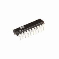
ATTINY261-20PU Atmel, ATTINY261-20PU Datasheet - Page 113

ATTINY261-20PU
Manufacturer Part Number
ATTINY261-20PU
Description
IC MCU AVR 2K FLASH 20MHZ 20-DIP
Manufacturer
Atmel
Series
AVR® ATtinyr
Specifications of ATTINY261-20PU
Core Processor
AVR
Core Size
8-Bit
Speed
20MHz
Connectivity
USI
Peripherals
Brown-out Detect/Reset, POR, PWM, WDT
Number Of I /o
16
Program Memory Size
2KB (1K x 16)
Program Memory Type
FLASH
Eeprom Size
128 x 8
Ram Size
128 x 8
Voltage - Supply (vcc/vdd)
2.7 V ~ 5.5 V
Data Converters
A/D 11x10b
Oscillator Type
Internal
Operating Temperature
-40°C ~ 85°C
Package / Case
20-DIP (0.300", 7.62mm)
Processor Series
ATTINY2x
Core
AVR8
Data Bus Width
8 bit
Data Ram Size
128 B
Interface Type
2-Wire/SPI/USI
Maximum Clock Frequency
20 MHz
Number Of Programmable I/os
16
Number Of Timers
2
Operating Supply Voltage
2.7 V to 5.5 V
Maximum Operating Temperature
+ 85 C
Mounting Style
Through Hole
3rd Party Development Tools
EWAVR, EWAVR-BL
Development Tools By Supplier
ATAVRDRAGON, ATSTK500, ATSTK600, ATAVRISP2, ATAVRONEKIT
Minimum Operating Temperature
- 40 C
On-chip Adc
11-ch x 10-bit
Data Rom Size
128 B
Height
4.95 mm
Length
26.92 mm
Supply Voltage (max)
5.5 V
Supply Voltage (min)
2.7 V
Width
7.11 mm
For Use With
ATSTK600 - DEV KIT FOR AVR/AVR32ATAVRBC100 - REF DESIGN KIT BATTERY CHARGER770-1007 - ISP 4PORT ATMEL AVR MCU SPI/JTAGATSTK505 - ADAPTER KIT FOR 14PIN AVR MCU
Lead Free Status / RoHS Status
Lead free / RoHS Compliant
Available stocks
Company
Part Number
Manufacturer
Quantity
Price
Company:
Part Number:
ATTINY261-20PU
Manufacturer:
ATMEL
Quantity:
256
- Current page: 113 of 242
- Download datasheet (5Mb)
2588E–AVR–08/10
Table 12-10
are set to Phase and Frequency Correct PWM Mode.
Table 12-10. Compare Output Mode, Phase and Frequency Correct PWM Mode
Table 12-11
are set to single-slope PWM6 Mode. In the PWM6 Mode the same Waveform Output (OCW1A)
is used for generating all waveforms and the Output Compare values OC1A and OC1A are con-
nected on thw all OC1x and OC1x pins as described below.
Table 12-11. Compare Output Mode, Single-Slope PWM6 Mode
Table 12-12
are set to dual-slope PWM6 Mode.I
Table 12-12. Compare Output Mode, Dual-Slope PWM6 Mode
Bits COM1A1 and COM1A0 are shadowed in TCCR1C. Writing to bits COM1A1 and COM1A0
will also change bits COM1A1S and COM1A0S in TCCR1C. Similary, changes written to bits
COM1A1S and COM1A0S in TCCR1C will show here. See
Register C” on page
COM1A1:0
COM1A1:0
COM1A1:0
00
01
10
11
00
01
10
11
00
01
10
11
shows the COM1A1:0 bit functionality when the PWM1A, WGM10 and WGM11 bits
shows the COM1A1:0 bit functionality when the PWM1A, WGM10 and WGM11 bits
shows the COM1A1:0 bit functionality when the PWM1A, WGM10 and WGM11 bits
OCW1A Behaviour
Normal port operation.
Cleared on Compare Match when up-counting.
Set on Compare Match when down-counting.
Cleared on Compare Match when up-counting.
Set on Compare Match when down-counting.
Set on Compare Match when up-counting.
Cleared on Compare Match when down-counting.
OCW1A Behaviour
Normal port operation.
Cleared on Compare Match.
Set when TCNT1 = 0x000.
Cleared on Compare Match.
Set when TCNT1 = 0x000.
Set on Compare Match.
Cleared when TCNT1 = 0x000.
OCW1A Behaviour
Normal port operation.
Cleared on Compare Match when up-counting.
Set on Compare Match when down-counting.
Cleared on Compare Match when up-counting.
Set on Compare Match when down-counting.
Set on Compare Match when up-counting.
Cleared on Compare Match when down-counting.
117.
“TCCR1C – Timer/Counter1 Control
OC1A Pin
Disconnected
OC1x Pin
Disconnected
OC1x Pin
Disconnected
Connected
Connected
Connected
OC1A
OC1A
OC1A
OC1A
OC1A
OC1A
OC1A Pin
Disconnected
Connected
Disconnected
Disconnected
OC1x Pin
Disconnected
OC1A
OC1A
OC1A
OC1x Pin
Disconnected
OC1A
OC1A
OC1A
113
Related parts for ATTINY261-20PU
Image
Part Number
Description
Manufacturer
Datasheet
Request
R

Part Number:
Description:
Manufacturer:
Atmel Corporation
Datasheet:

Part Number:
Description:
Manufacturer:
Atmel Corporation
Datasheet:

Part Number:
Description:
IC MCU AVR 2K FLASH 20MHZ 32-QFN
Manufacturer:
Atmel
Datasheet:

Part Number:
Description:
MCU AVR 2K FLASH 15MHZ 32-QFN
Manufacturer:
Atmel
Datasheet:

Part Number:
Description:
MCU AVR 2KB FLASH 15MHZ 32-VQFN
Manufacturer:
Atmel
Datasheet:

Part Number:
Description:
IC MCU AVR 2K FLASH 20MHZ 20SOIC
Manufacturer:
Atmel
Datasheet:

Part Number:
Description:
Attiny261 8-bit Microcontroller With 2/4/8k Bytes In-system Programmable Flash
Manufacturer:
ATMEL Corporation
Datasheet:

Part Number:
Description:
IC MCU AVR 2K FLASH 20MHZ 20SOIC
Manufacturer:
Atmel
Datasheet:

Part Number:
Description:
IC MCU AVR 2K FLASH 20MHZ 32QFN
Manufacturer:
Atmel
Datasheet:

Part Number:
Description:
Manufacturer:
Atmel Corporation
Datasheet:


