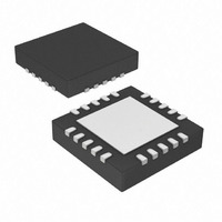
PIC18F14K22-I/ML Microchip Technology, PIC18F14K22-I/ML Datasheet - Page 351

PIC18F14K22-I/ML
Manufacturer Part Number
PIC18F14K22-I/ML
Description
IC PIC MCU FLASH 512KX16 20-QFN
Manufacturer
Microchip Technology
Series
PIC® XLP™ 18Fr
Datasheets
1.PIC16F722-ISS.pdf
(8 pages)
2.PIC18LF13K22-ISS.pdf
(388 pages)
3.PIC18LF13K22-ISS.pdf
(12 pages)
4.PIC18LF13K22-ISS.pdf
(36 pages)
5.PIC18F13K22-ISS.pdf
(382 pages)
Specifications of PIC18F14K22-I/ML
Core Size
8-Bit
Program Memory Size
16KB (8K x 16)
Core Processor
PIC
Speed
64MHz
Connectivity
I²C, LIN, SPI, UART/USART
Peripherals
Brown-out Detect/Reset, POR, PWM, WDT
Number Of I /o
17
Program Memory Type
FLASH
Eeprom Size
256 x 8
Ram Size
512 x 8
Voltage - Supply (vcc/vdd)
1.8 V ~ 5.5 V
Data Converters
A/D 12x10b
Oscillator Type
Internal
Operating Temperature
-40°C ~ 85°C
Package / Case
20-VQFN Exposed Pad, 20-HVQFN, 20-SQFN, 20-DHVQFN
Controller Family/series
PIC18
No. Of I/o's
18
Eeprom Memory Size
256Byte
Ram Memory Size
512Byte
Cpu Speed
64MHz
No. Of Timers
4
Processor Series
PIC18F
Core
PIC
Data Bus Width
8 bit
Data Ram Size
512 B
Interface Type
I2C, MSSP, SPI, USART
Maximum Clock Frequency
64 MHz
Number Of Programmable I/os
17
Number Of Timers
4
Operating Supply Voltage
1.8 V to 5.5 V
Maximum Operating Temperature
+ 125 C
Mounting Style
SMD/SMT
3rd Party Development Tools
52715-96, 52716-328, 52717-734, 52712-325, EWPIC18
Development Tools By Supplier
PG164130, DV164035, DV244005, DV164005
Minimum Operating Temperature
- 40 C
On-chip Adc
10 bit, 12 Channel
Package
20QFN EP
Device Core
PIC
Family Name
PIC18
Maximum Speed
64 MHz
A/d Bit Size
10 bit
A/d Channels Available
12
Height
0.88 mm
Length
4 mm
Supply Voltage (max)
5.5 V
Supply Voltage (min)
1.8 V, 2.7 V
Width
4 mm
Lead Free Status / RoHS Status
Lead free / RoHS Compliant
Lead Free Status / RoHS Status
Lead free / RoHS Compliant, Lead free / RoHS Compliant
Available stocks
Company
Part Number
Manufacturer
Quantity
Price
Part Number:
PIC18F14K22-I/ML
Manufacturer:
MICROCHIP/微芯
Quantity:
20 000
- PIC16F722-ISS PDF datasheet
- PIC18LF13K22-ISS PDF datasheet #2
- PIC18LF13K22-ISS PDF datasheet #3
- PIC18LF13K22-ISS PDF datasheet #4
- PIC18F13K22-ISS PDF datasheet #5
- Current page: 351 of 382
- Download datasheet (6Mb)
FIGURE 25-14:
TABLE 25-9:
© 2009 Microchip Technology Inc.
130
131
132
135
TBD
Legend: TBD = To Be Determined
Note 1:
Param
No.
2:
3:
4:
A/D DATA
Note 1:
SAMPLE
A/D CLK
T
T
T
T
T
ADRES
Symbol
BSF ADCON0, GO
AD
CNV
ACQ
SWC
DIS
ADIF
The time of the A/D clock period is dependent on the device frequency and the T
ADRES register may be read on the following T
The time for the holding capacitor to acquire the “New” input voltage when the voltage changes full scale
after the conversion (V
Ω.
On the following cycle of the device clock.
GO
2:
Q4
If the A/D clock source is selected as RC, a time of T
This allows the SLEEP instruction to be executed.
This is a minimal RC delay (typically 100 ns), which also disconnects the holding capacitor from the analog input.
A/D CONVERSION REQUIREMENTS
A/D Clock Period
Conversion Time
(not including acquisition time)
Acquisition Time
Switching Time from Convert → Sample
Discharge Time
132
A/D CONVERSION TIMING
(Note 2)
Characteristic
DD
(3)
9
to V
SS
8
or V
OLD_DATA
SS
(2)
7
Preliminary
to V
.. .
SAMPLING STOPPED
DD
PIC18F1XK22/LF1XK22
CY
). The source impedance (R
CY
is added before the A/D clock starts.
cycle.
. . .
131
130
Min.
TBD
TBD
0.7
0.7
1.4
0.2
11
—
2
(Note 4)
25.0
4.0
Max.
12
—
—
—
1
(1)
(1)
1
Units
T
μs
μs
μs
μs
μs
μs
AD
S
) on the input channels is 50
0
T
-40°C to 85°C
T
≤ 125°C
A/D RC mode
-40°C to +85°C
0°C ≤ to ≤ +85°C
OSC
OSC
AD
based, V
based, V
clock divider.
NEW_DATA
DONE
Conditions
DS41365B-page 349
T
CY
REF
REF
≥ 3.0V to
≥ 3.0V,
Related parts for PIC18F14K22-I/ML
Image
Part Number
Description
Manufacturer
Datasheet
Request
R

Part Number:
Description:
Manufacturer:
Microchip Technology Inc.
Datasheet:

Part Number:
Description:
Manufacturer:
Microchip Technology Inc.
Datasheet:

Part Number:
Description:
Manufacturer:
Microchip Technology Inc.
Datasheet:

Part Number:
Description:
Manufacturer:
Microchip Technology Inc.
Datasheet:

Part Number:
Description:
Manufacturer:
Microchip Technology Inc.
Datasheet:

Part Number:
Description:
Manufacturer:
Microchip Technology Inc.
Datasheet:

Part Number:
Description:
Manufacturer:
Microchip Technology Inc.
Datasheet:

Part Number:
Description:
Manufacturer:
Microchip Technology Inc.
Datasheet:


