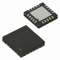
ATTINY2313V-10MU Atmel, ATTINY2313V-10MU Datasheet - Page 18

ATTINY2313V-10MU
Manufacturer Part Number
ATTINY2313V-10MU
Description
10MHZ MLF IND TEMP GREEN
Manufacturer
Atmel
Series
AVR® ATtinyr
Datasheets
1.ATTINY2313-20MU.pdf
(226 pages)
2.ATTINY2313V-10MU.pdf
(15 pages)
3.ATTINY2313V-10SU.pdf
(20 pages)
Specifications of ATTINY2313V-10MU
Core Processor
AVR
Core Size
8-Bit
Speed
10MHz
Connectivity
SPI, UART/USART
Peripherals
Brown-out Detect/Reset, POR, PWM, WDT
Number Of I /o
18
Program Memory Size
2KB (1K x 16)
Program Memory Type
FLASH
Eeprom Size
128 x 8
Ram Size
128 x 8
Voltage - Supply (vcc/vdd)
1.8 V ~ 5.5 V
Oscillator Type
Internal
Operating Temperature
-40°C ~ 85°C
Package / Case
20-MLF®, QFN
Processor Series
ATTINY2x
Core
AVR8
Data Bus Width
8 bit
Data Ram Size
128 B
Interface Type
SPI/UART/USI
Maximum Clock Frequency
10 MHz
Number Of Programmable I/os
18
Number Of Timers
2
Operating Supply Voltage
1.8 V to 5.5 V
Maximum Operating Temperature
+ 85 C
Mounting Style
SMD/SMT
Minimum Operating Temperature
- 40 C
For Use With
ATSTK600-DIP40 - STK600 SOCKET/ADAPTER 40-PDIP770-1007 - ISP 4PORT ATMEL AVR MCU SPI/JTAGATAVRDRAGON - KIT DRAGON 32KB FLASH MEM AVRATAVRISP2 - PROGRAMMER AVR IN SYSTEMATJTAGICE2 - AVR ON-CHIP D-BUG SYSTEM
Lead Free Status / RoHS Status
Lead free / RoHS Compliant
Data Converters
-
Lead Free Status / Rohs Status
Lead free / RoHS Compliant
Other names
Q2312268B
Available stocks
Company
Part Number
Manufacturer
Quantity
Price
Part Number:
ATTINY2313V-10MU
Manufacturer:
ATMEL/爱特梅尔
Quantity:
20 000
Atomic Byte
Programming
Split Byte
Programming
Erase
Write
18
ATtiny2313
• Bit 2 – EEMPE: EEPROM Master Program Enable
The EEMPE bit determines whether writing EEPE to one will have effect or not.
When EEMPE is set, setting EEPE within four clock cycles will program the EEPROM at the
selected address. If EEMPE is zero, setting EEPE will have no effect. When EEMPE has been
written to one by software, hardware clears the bit to zero after four clock cycles.
• Bit 1 – EEPE: EEPROM Program Enable
The EEPROM Program Enable Signal EEPE is the programming enable signal to the EEPROM.
When EEPE is written, the EEPROM will be programmed according to the EEPMn bits setting.
The EEMPE bit must be written to one before a logical one is written to EEPE, otherwise no
EEPROM write takes place. When the write access time has elapsed, the EEPE bit is cleared by
hardware. When EEPE has been set, the CPU is halted for two cycles before the next instruction
is executed.
• Bit 0 – EERE: EEPROM Read Enable
The EEPROM Read Enable Signal – EERE – is the read strobe to the EEPROM. When the cor-
rect address is set up in the EEAR Register, the EERE bit must be written to one to trigger the
EEPROM read. The EEPROM read access takes one instruction, and the requested data is
available immediately. When the EEPROM is read, the CPU is halted for four cycles before the
next instruction is executed. The user should poll the EEPE bit before starting the read opera-
tion. If a write operation is in progress, it is neither possible to read the EEPROM, nor to change
the EEAR Register.
Using Atomic Byte Programming is the simplest mode. When writing a byte to the EEPROM, the
user must write the address into the EEAR Register and data into EEDR Register. If the EEPMn
bits are zero, writing EEPE (within four cycles after EEMPE is written) will trigger the erase/write
operation. Both the erase and write cycle are done in one operation and the total programming
time is given in Table 1. The EEPE bit remains set until the erase and write operations are com-
pleted. While the device is busy with programming, it is not possible to do any other EEPROM
operations.
It is possible to split the erase and write cycle in two different operations. This may be useful if
the system requires short access time for some limited period of time (typically if the power sup-
ply voltage falls). In order to take advantage of this method, it is required that the locations to be
written have been erased before the write operation. But since the erase and write operations
are split, it is possible to do the erase operations when the system allows doing time-consuming
operations (typically after Power-up).
To erase a byte, the address must be written to EEAR. If the EEPMn bits are 0b01, writing the
EEPE (within four cycles after EEMPE is written) will trigger the erase operation only (program-
ming time is given in Table 1). The EEPE bit remains set until the erase operation completes.
While the device is busy programming, it is not possible to do any other EEPROM operations.
To write a location, the user must write the address into EEAR and the data into EEDR. If the
EEPMn bits are 0b10, writing the EEPE (within four cycles after EEMPE is written) will trigger
the write operation only (programming time is given in Table 1). The EEPE bit remains set until
the write operation completes. If the location to be written has not been erased before write, the
data that is stored must be considered as lost. While the device is busy with programming, it is
not possible to do any other EEPROM operations.
The calibrated Oscillator is used to time the EEPROM accesses. Make sure the Oscillator fre-
quency is within the requirements described in
page
26.
“Oscillator Calibration Register – OSCCAL” on
2543L–AVR–08/10


