ATTINY24-20MU Atmel, ATTINY24-20MU Datasheet
ATTINY24-20MU
Specifications of ATTINY24-20MU
Available stocks


Related parts for ATTINY24-20MU


ATTINY24-20MU Summary of contents
Page 1
... I/O and Packages – Available in 20-Pin QFN/MLF & 14-Pin SOIC and PDIP – Twelve Programmable I/O Lines • Operating Voltage: – 1.8 – 5.5V for ATtiny24V/44V/84V – 2.7 – 5.5V for ATtiny24/44/84 • Speed Grade – ATtiny24V/44V/84V • 0 – 4 MHz @ 1.8 – 5.5V • ...
Page 2
... Pin Configurations Figure 1-1. Pinout ATtiny24/44/84 (PCINT8/XTAL1/CLKI) PB0 (PCINT9/XTAL2) PB1 (PCINT11/RESET/dW) PB3 (PCINT10/INT0/OC0A/CKOUT) PB2 (PCINT7/ICP/OC0B/ADC7) PA7 (PCINT6/OC1A/SDA/MOSI/DI/ADC6) PA6 (ADC4/USCK/SCL/T1/PCINT4) PA4 (ADC3/T0/PCINT3) PA3 (ADC2/AIN1/PCINT2) PA2 (ADC1/AIN0/PCINT1) PA1 (ADC0/AREF/PCINT0) PA0 NOTE Bottom pad should be soldered to ground. DNC: Do Not Connect 1.1 Pin Descriptions 1.1.1 VCC Supply voltage ...
Page 3
... Port B also serves the functions of various special features of the ATtiny24/44/84 as listed in Section 10.2 “Alternate Port Functions” on page 1.1.4 RESET Reset input. A low level on this pin for longer than the minimum pulse length will generate a reset, even if the clock is not running and provided the reset pin has not been disabled. The min- imum pulse length is given in generate a reset ...
Page 4
... Overview ATtiny24/44/ low-power CMOS 8-bit microcontroller based on the AVR enhanced RISC architecture. By executing powerful instructions in a single clock cycle, the ATtiny24/44/84 achieves throughputs approaching 1 MIPS per MHz allowing the system designer to optimize power consumption versus processing speed. Figure 2-1. VCC GND The AVR core combines a rich instruction set with 32 general purpose working registers ...
Page 5
... ISP Flash allows the Program memory to be re-programmed in-system through an SPI serial interface conventional non-volatile memory programmer on-chip boot code running on the AVR core. The ATtiny24/44/84 AVR is supported with a full suite of program and system development tools including: C Compilers, Macro Assemblers, Program Debugger/Simulators and Evaluation kits. 8006KS–AVR–10/10 ...
Page 6
... Reliability Qualification results show that the projected data retention failure rate is much less than 1 PPM over 20 years at 85°C or 100 years at 25°C. 3.4 Disclaimer Typical values contained in this datasheet are based on simulations and characterization of other AVR microcontrollers manufactured on the same process technology. ATtiny24/44/84 6 8006KS–AVR–10/10 ...
Page 7
... ADATE ADIF ADIE ADC Data Register High Byte ADC Data Register Low Byte ACME – ADLAR – – ADC6D ADC5D ADC4D ADC3D – – – PRTIM1 ATtiny24/44/84 Bit 2 Bit 1 Bit – SP9 SP8 SP2 SP1 SP0 – – – – – ...
Page 8
... Some of the Status Flags are cleared by writing a logical one to them. Note that, unlike most other AVRs, the CBI and SBI instructions will only operation the specified bit, and can therefore be used on registers containing such Status Flags. The CBI and SBI instructions work with registers 0x00 to 0x1F only. ATtiny24/44/84 8 8006KS–AVR–10/10 ...
Page 9
... PC ← then PC ← then PC ← then PC ← then PC ← then PC ← I/O(P,b) ← 1 I/O(P,b) ← 0 Rd(n+1) ← Rd(n), Rd(0) ← 0 Rd(n) ← Rd(n+1), Rd(7) ← 0 Rd(0)←C,Rd(n+1)← Rd(n),C←Rd(7) ATtiny24/44/84 Operation Flags #Clocks Z,C,N,V,H Z,C,N,V,H Z,C,N,V,S Z,C,N,V,H Z,C,N,V,H Z,C,N,V,H Z,C,N,V,H ...
Page 10
... Rd Pop Register from Stack MCU CONTROL INSTRUCTIONS NOP No Operation SLEEP Sleep WDR Watchdog Reset BREAK Break ATtiny24/44/84 10 Description Rd(7)←C,Rd(n)← Rd(n+1),C←Rd(0) Rd(n) ← Rd(n+1), n=0..6 Rd(3..0)←Rd(7..4),Rd(7..4)←Rd(3..0) SREG(s) ← 1 SREG(s) ← ← Rr(b) Rd(b) ← ← ← ← ...
Page 11
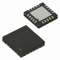
... Ordering Code Package ATtiny24V-10SSU 14S1 ATtiny24V-10SSUR 14S1 ATtiny24V-10PU 14P3 ATtiny24V-10MU 20M1 ATtiny24V-10MUR 20M1 ATtiny24-20SSU 14S1 ATtiny24-20SSUR 14S1 ATtiny24-20PU 14P3 ATtiny24-20MU 20M1 ATtiny24-20MUR 20M1 Package Type ATtiny24/44/84 (2) Operational Range Industrial (3) (-40°C to +85°C) Industrial (3) (-40°C to +85°C) 11 ...
Page 12
... Wide Body, Plastic Gull Wing Small Outline Package (SOIC) 14P3 14-lead, 0.300" Wide, Plastic Dual Inline Package (PDIP) 20M1 20-pad 0.8 mm Body, Quad Flat No-Lead/Micro Lead Frame Package (QFN/MLF) ATtiny24/44/84 12 (1) Ordering Code Package ATtiny44V-10SSU 14S1 ...
Page 13
... Ordering Code Package ATtiny84V-10SSU 14S1 ATtiny84V-10SSUR 14S1 ATtiny84V-10PU 14P3 ATtiny84V-10MU 20M1 ATtiny84V-10MUR 20M1 ATtiny84-20SSU 14S1 ATtiny84-20SSUR 14S1 ATtiny84-20PU 14P3 ATtiny84-20MU 20M1 ATtiny84-20MUR 20M1 Package Type ATtiny24/44/84 (2) Operational Range Industrial (3) (-40°C to +85°C) Industrial (3) (-40°C to +85°C) 13 ...
Page 14
... TOP VIEW D2 Pin #1 Notch (0. BOTTOM VIEW Reference JEDEC Standard MO-220, Fig. 1 (SAW Singulation) WGGD-5. Note: 2325 Orchard Parkway San Jose, CA 95131 R ATtiny24/44/ TITLE 20M1, 20-pad 0.8 mm Body, Lead Pitch 0.50 mm, 2.6 mm Exposed Pad, Micro Lead Frame Package (MLF) SIDE VIEW A2 ...
Page 15
... Mold Flash or Protrusion shall not exceed 0.25 mm (0.010"). 2325 Orchard Parkway San Jose, CA 95131 R 8006KS–AVR–10/10 D PIN TITLE 14P3, 14-lead (0.300"/7.62 mm Wide) Plastic Dual Inline Package (PDIP) ATtiny24/44/ COMMON DIMENSIONS (Unit of Measure = mm) SYMBOL MIN NOM A – – A1 0.381 – D 18.669 – ...
Page 16
... Dimension E does not include inter-lead Flash or protrusion. Inter-lead flash and protrusions shall not exceed 0.25 mm (0.010") per side the length of the terminal for soldering to a substrate. 5. The lead width B, as measured 0.36 mm (0.014") or greater above the seating plane, shall not exceed a maximum value of 0.61 mm (0.024") per side. 2325 Orchard Parkway San Jose, CA 95131 R ATtiny24/44/ SYMBOL ...
Page 17
... Errata The revision letters in this section refer to the revision of the corresponding ATtiny24/44/84 device. 8.1 ATtiny24 8.1.1 Rev. D – known errata. 8.1.2 Rev. C • Reading EEPROM when system clock frequency is below 900 kHz may not work 1. Reading EEPROM when system clock frequency is below 900 kHz may not work Reading data from the EEPROM at system clock frequency below 900 kHz may result in wrong data read ...
Page 18
... Reading EEPROM when system clock frequency is below 900 kHz may not work Reading data from the EEPROM at system clock frequency below 900 kHz may result in wrong data read. Problem Fix/Work around Avoid using the EEPROM at clock frequency below 900 kHz. ATtiny24/44/84 18 8006KS–AVR–10/10 ...
Page 19
... ATtiny84 8.3.1 Rev. A – known errata. 8006KS–AVR–10/10 ATtiny24/44/84 19 ...
Page 20
... Added Table: – 8. Updated Figure: – 9. Updated old and Hysteresis”. 10. Changed ATtiny24/44 device status to “Not Recommended for New Designs. Use: ATtiny24A/44A”. ATtiny24/44/84 20 Section 24. “Ordering Information” on page Section 6.4 “Clock Output Buffer” on page Table 19-16, “High-voltage Serial Programming Instruction Set for 171. Table 6-8, “ ...
Page 21
... Characteristics” on page 176 “Accuracy of Calibrated Internal RC Oscillator” on page 176 “System and Reset Characteristics” on page 177 “Supply Current of I/O Modules” on page 185 “ATtiny24” on page 223 “ATtiny44” on page 224 “ATtiny84” on page 225 “MCUCR – MCU Control Register” on page 36 “ ...
Page 22
... CC (Reset Pin Used as I/O)” on page 203 CC ” on page 205 CC ” on page 206 CC ” on page 207 CC (ATtiny24)” on page 209 CC (ATtiny44)” on page 209 CC (ATtiny84)” on page 210 CC = 3V)” on page 198 CC = 5V)” on page 198 CC = 3V)” on page 199 CC = 5V)” ...
Page 23
... Table 11-8 on page 83, Table 20-11 on page Updated table references in “TCCR0A – Timer/Counter Control Register A” on page Updated Port B, Bit 0 functions in Updated WDTCR bit name to WDTCSR in assembly code examples. ATtiny24/44/84 = -40°C to +85°C” -40°C to +85° 1.8 - 5.5V (Unless 25° (Unless ...
Page 24
... Updated Features in 5. Updated Operation in 6. Updated ATtiny24/44/84 24 “TIFR1 – Timer/Counter Interrupt Flag Register 1” on page “TIFR1 – Timer/Counter Interrupt Flag Register 1” on page “SPI Master Operation Example” on page “Enter High-voltage Serial Programming Mode” on page “Electrical Characteristics” on page “ ...
Page 25
... Rev A. 12/05 Initial revision. 8006KS–AVR–10/10 Updated DC Characteristics in “Electrical Characteristics” on page Updated “Typical Characteristics” on page Updated “Errata” on page 223. ATtiny24/44/84 174. 185. 25 ...
Page 26
... Disclaimer: The information in this document is provided in connection with Atmel products. No license, express or implied, by estoppel or otherwise, to any intellectual property right is granted by this document or in connection with the sale of Atmel products. EXCEPT AS SET FORTH IN ATMEL’S TERMS AND CONDI- TIONS OF SALE LOCATED ON ATMEL’S WEB SITE, ATMEL ASSUMES NO LIABILITY WHATSOEVER AND DISCLAIMS ANY EXPRESS, IMPLIED OR STATUTORY WARRANTY RELATING TO ITS PRODUCTS INCLUDING, BUT NOT LIMITED TO, THE IMPLIED WARRANTY OF MERCHANTABILITY, FITNESS FOR A PARTICULAR PURPOSE, OR NON-INFRINGEMENT ...