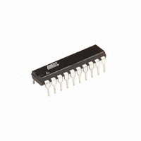
AT89LP2052-20PU Atmel, AT89LP2052-20PU Datasheet - Page 77

AT89LP2052-20PU
Manufacturer Part Number
AT89LP2052-20PU
Description
IC 8051 MCU FLASH 2K 20DIP
Manufacturer
Atmel
Series
89LPr
Datasheet
1.AT89LP2052-20PU.pdf
(94 pages)
Specifications of AT89LP2052-20PU
Core Processor
8051
Core Size
8-Bit
Speed
20MHz
Connectivity
SPI, UART/USART
Peripherals
Brown-out Detect/Reset, POR, PWM, WDT
Number Of I /o
15
Program Memory Size
2KB (2K x 8)
Program Memory Type
FLASH
Ram Size
256 x 8
Voltage - Supply (vcc/vdd)
2.4 V ~ 5.5 V
Oscillator Type
Internal
Operating Temperature
-40°C ~ 85°C
Package / Case
20-DIP (0.300", 7.62mm)
Processor Series
AT89x
Core
8051
Data Bus Width
8 bit
Data Ram Size
256 B
Interface Type
SPI/UART
Maximum Clock Frequency
20 MHz
Number Of Programmable I/os
15
Number Of Timers
2
Operating Supply Voltage
2.4 V to 5.5 V
Maximum Operating Temperature
+ 85 C
Mounting Style
Through Hole
3rd Party Development Tools
PK51, CA51, A51, ULINK2
Development Tools By Supplier
AT89ISP
Minimum Operating Temperature
- 40 C
Package
20PDIP
Device Core
8051
Family Name
AT89
Maximum Speed
20 MHz
Cpu Family
AT89
Device Core Size
8b
Frequency (max)
20MHz
Total Internal Ram Size
256Byte
# I/os (max)
15
Number Of Timers - General Purpose
2
Operating Supply Voltage (typ)
2.5/3.3/5V
Operating Supply Voltage (max)
5.5V
Operating Supply Voltage (min)
2.4V
Instruction Set Architecture
CISC
Operating Temp Range
-40C to 85C
Operating Temperature Classification
Industrial
Mounting
Through Hole
Pin Count
20
Package Type
PDIP
Lead Free Status / RoHS Status
Lead free / RoHS Compliant
Eeprom Size
-
Data Converters
-
Lead Free Status / Rohs Status
Lead free / RoHS Compliant
Available stocks
Company
Part Number
Manufacturer
Quantity
Price
Company:
Part Number:
AT89LP2052-20PU
Manufacturer:
ON
Quantity:
340
23.5.6
Figure 23-27. ISP Command Sequence
Table 23-4.
3547J–MICRO–10/09
Symbol
t
t
t
t
t
t
t
t
t
t
t
SHSL
SLSH
t
t
WRC
t
SOH
SCK
t
SOV
SOE
SOX
SSE
SSD
ERS
SIS
SIH
SR
SF
MOSI
MISO
SCK
ISP Command Sequence
SS
Serial Programming Interface Parameters
Parameter
Serial Clock Cycle Time
Clock High Time
Clock Low Time
Rise Time
Fall Time
Serial Input Setup Time
Serial Input Hold Time
Serial Output Hold Time
Serial Output Valid Time
Output Enable Time
Output Disable Time
SS Enable Lead Time
SS Disable Lag Time
Wire Cycle Time
Erase Cycle Time
The ISP multi-byte command sequence is shown in
Preamble
• SS should be brought low before the first byte in a command is sent and brought back high
• Command bytes are issued serially on MOSI (P1.5).
• Data bytes are output serially on MISO (P1.6).
after the final byte in the command has been sent. The command is not complete until SS
returns high.
X
7
6 5 4 3 2 1
Opcode
X
0
7
6 5 4 3 2 1
Address High
X
Min
200
100
100
100
50
10
10
0
7
Figure
6 5 4 3 2 1
Address Low
AT89LP2052/LP4052
X
23-27.
Max
4.5
25
25
10
35
10
25
9
0
7
7
6 5 4 3 2 1
6 5 4 3 2 1
Data Out
Data In
Units
ms
ms
0
0
ns
ns
ns
ns
ns
ns
ns
ns
ns
ns
ns
ns
ns
77


