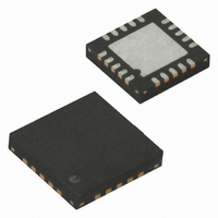
ATTINY13V-10MU Atmel, ATTINY13V-10MU Datasheet - Page 69

ATTINY13V-10MU
Manufacturer Part Number
ATTINY13V-10MU
Description
IC MCU AVR 1K FLASH 10MHZ 20MLF
Manufacturer
Atmel
Series
AVR® ATtinyr
Specifications of ATTINY13V-10MU
Core Processor
AVR
Core Size
8-Bit
Speed
10MHz
Peripherals
Brown-out Detect/Reset, POR, PWM, WDT
Number Of I /o
6
Program Memory Size
1KB (512 x 16)
Program Memory Type
FLASH
Eeprom Size
64 x 8
Ram Size
64 x 8
Voltage - Supply (vcc/vdd)
1.8 V ~ 5.5 V
Data Converters
A/D 4x10b
Oscillator Type
Internal
Operating Temperature
-40°C ~ 85°C
Package / Case
20-MLF®, QFN
Processor Series
ATTINY1x
Core
AVR8
Data Bus Width
8 bit
Data Ram Size
64 B
Interface Type
SPI
Maximum Clock Frequency
10 MHz
Number Of Programmable I/os
6
Number Of Timers
1
Operating Supply Voltage
1.8 V to 5.5 V
Maximum Operating Temperature
+ 85 C
Mounting Style
SMD/SMT
Minimum Operating Temperature
- 40 C
On-chip Adc
4-ch x 10-bit
Package
20MLF EP
Device Core
AVR
Family Name
ATtiny
Maximum Speed
10 MHz
For Use With
ATSTK600-DIP40 - STK600 SOCKET/ADAPTER 40-PDIP770-1007 - ISP 4PORT ATMEL AVR MCU SPI/JTAGATAVRDRAGON - KIT DRAGON 32KB FLASH MEM AVRATAVRISP2 - PROGRAMMER AVR IN SYSTEMATJTAGICE2 - AVR ON-CHIP D-BUG SYSTEM
Lead Free Status / RoHS Status
Lead free / RoHS Compliant
Connectivity
-
Lead Free Status / Rohs Status
Lead free / RoHS Compliant
Available stocks
Company
Part Number
Manufacturer
Quantity
Price
Company:
Part Number:
ATTINY13V-10MU
Manufacturer:
Atmel
Quantity:
10
11.9
11.9.1
2535J–AVR–08/10
Register Description
TCCR0A – Timer/Counter Control Register A
Figure 11-11. Timer/Counter Timing Diagram, Clear Timer on Compare Match mode, with Pres-
• Bits 7:6 – COM01A:0: Compare Match Output A Mode
These bits control the Output Compare pin (OC0A) behavior. If one or both of the COM0A1:0
bits are set, the OC0A output overrides the normal port functionality of the I/O pin it is connected
to. However, note that the Data Direction Register (DDR) bit corresponding to the OC0A pin
must be set in order to enable the output driver.
When OC0A is connected to the pin, the function of the COM0A1:0 bits depends on the
WGM02:0 bit setting.
Table 11-2
CTC mode (non-PWM).
Table 11-2.
Table 11-3 on page 70
fast PWM mode.
TCNTn
(clk
OCRnx
(CTC)
OCFnx
Bit
Read/Write
Initial Value
clk
clk
I/O
COM01
I/O
Tn
/8)
0
0
1
1
shows the COM0A1:0 bit functionality when the WGM02:0 bits are set to a normal or
caler (f
Compare Output Mode, non-PWM Mode
COM0A1
R/W
7
0
COM00
0
1
0
1
clk_I/O
TOP - 1
shows the COM0A1:0 bit functionality when the WGM01:0 bits are set to
COM0A0
R/W
/8)
6
0
Description
Normal port operation, OC0A disconnected.
Toggle OC0A on Compare Match
Clear OC0A on Compare Match
Set OC0A on Compare Match
COM0B1
R/W
5
0
COM0B0
R/W
TOP
4
0
TOP
3
R
0
–
R
BOTTOM
2
–
0
WGM01
R/W
1
0
WGM00
R/W
0
0
BOTTOM + 1
TCCR0A
69


