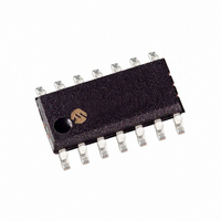
PIC16F684-I/SL Microchip Technology, PIC16F684-I/SL Datasheet - Page 65

PIC16F684-I/SL
Manufacturer Part Number
PIC16F684-I/SL
Description
IC PIC MCU FLASH 2KX14 14SOIC
Manufacturer
Microchip Technology
Series
PIC® 16Fr
Datasheets
1.PIC16F616T-ISL.pdf
(8 pages)
2.PIC16F688T-ISL.pdf
(688 pages)
3.PIC16F684-ISL.pdf
(4 pages)
4.PIC16F684-ISL.pdf
(192 pages)
5.PIC16F684-ISL.pdf
(6 pages)
6.PIC16F684-IST.pdf
(164 pages)
Specifications of PIC16F684-I/SL
Program Memory Type
FLASH
Program Memory Size
3.5KB (2K x 14)
Package / Case
14-SOIC (3.9mm Width), 14-SOL
Core Processor
PIC
Core Size
8-Bit
Speed
20MHz
Peripherals
Brown-out Detect/Reset, POR, PWM, WDT
Number Of I /o
12
Eeprom Size
256 x 8
Ram Size
128 x 8
Voltage - Supply (vcc/vdd)
2 V ~ 5.5 V
Data Converters
A/D 8x10b
Oscillator Type
Internal
Operating Temperature
-40°C ~ 85°C
Processor Series
PIC16F
Core
PIC
Data Bus Width
8 bit
Data Ram Size
128 B
Maximum Clock Frequency
20 MHz
Number Of Programmable I/os
12
Number Of Timers
3
Operating Supply Voltage
2 V to 5.5 V
Maximum Operating Temperature
+ 85 C
Mounting Style
SMD/SMT
3rd Party Development Tools
52715-96, 52716-328, 52717-734
Development Tools By Supplier
PG164130, DV164035, DV244005, DV164005, PG164120, ICE2000, DM163014, DM164120-4
Minimum Operating Temperature
- 40 C
On-chip Adc
8-ch x 10-bit
Package
14SOIC N
Device Core
PIC
Family Name
PIC16
Maximum Speed
20 MHz
Data Rom Size
256 B
Height
1.25 mm
Length
8.65 mm
Supply Voltage (max)
5.5 V
Supply Voltage (min)
2 V
Width
3.9 mm
Lead Free Status / RoHS Status
Lead free / RoHS Compliant
Connectivity
-
Lead Free Status / Rohs Status
Lead free / RoHS Compliant
Other names
PIC16F684-I/SLG
Available stocks
Company
Part Number
Manufacturer
Quantity
Price
Company:
Part Number:
PIC16F684-I/SL
Manufacturer:
MXIC
Quantity:
1 500
Company:
Part Number:
PIC16F684-I/SL
Manufacturer:
Microchip Technology
Quantity:
32 570
Part Number:
PIC16F684-I/SL
Manufacturer:
MICROCHIP/微芯
Quantity:
20 000
9.0
The Analog-to-Digital converter (A/D) allows conver-
sion of an analog input signal to a 10-bit binary repre-
sentation of that signal. The PIC16F684 has eight
analog inputs, multiplexed into one sample and hold
FIGURE 9-1:
9.1
There are three registers available to control the
functionality of the A/D module:
1.
2.
3.
9.1.1
The ANS<7:0> bits (ANSEL<7:0>) and the TRIS bits
control the operation of the A/D port pins. Set the
corresponding TRIS bits to set the pin output driver to
its high-impedance state. Likewise, set the correspond-
ing ANSEL bit to disable the digital input buffer.
9.1.2
There are eight analog channels on the PIC16F684,
AN0
(ADCON0<4:2>) control which channel is connected to
the sample and hold circuit.
2004 Microchip Technology Inc.
Note:
ANSEL (Register 9-1)
ADCON0 (Register 9-2)
ADCON1 (Register 9-3)
through
ANALOG-TO-DIGITAL
CONVERTER (A/D) MODULE
A/D Configuration and Operation
ANALOG PORT PINS
Analog voltages on any pin that is defined
as a digital input may cause the input
buffer to conduct excess current.
CHANNEL SELECTION
RA1/AN1/V
AN7.
A/D BLOCK DIAGRAM
RC0/AN4
RC1/AN5
RC2/AN6
RC3/AN7
RA4/AN3
RA0/AN0
RA2/AN2
REF
The
CHS<2:0>
CHS<2:0>
V
REF
Preliminary
bits
V
DD
GO/DONE
VCFG = 0
VCFG = 1
ADON
circuit. The output of the sample and hold is connected
to the input of the converter. The converter generates a
binary result via successive approximation and stores
the result in a 10-bit register. The voltage reference
used in the conversion is software selectable to either
V
shows the block diagram of the A/D on the PIC16F684.
9.1.3
There are two options for the voltage reference to the
A/D converter: either V
applied to V
controls the voltage reference selection. If VCFG is set,
then the voltage on the V
otherwise, V
V
DD
SS
or a voltage applied by the V
A/D
ADFM
VOLTAGE REFERENCE
REF
DD
is the reference.
is used. The VCFG bit (ADCON0<6>)
ADRESH ADRESL
DD
is used, or an analog voltage
PIC16F684
10
10
REF
pin is the reference;
REF
DS41202C-page 63
pin. Figure 9-1


