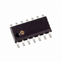
PIC16F630-I/SL Microchip Technology, PIC16F630-I/SL Datasheet - Page 11

PIC16F630-I/SL
Manufacturer Part Number
PIC16F630-I/SL
Description
IC MCU FLASH 1KX14 EEPROM 14SOIC
Manufacturer
Microchip Technology
Series
PIC® 16Fr
Datasheets
1.PIC16F616T-ISL.pdf
(8 pages)
2.PIC12F629T-ISN.pdf
(24 pages)
3.PIC16F630-ISL.pdf
(132 pages)
4.PIC16F630-ISL.pdf
(2 pages)
5.PIC16F630-ISL.pdf
(10 pages)
6.PIC16F676-EP.pdf
(132 pages)
7.PIC16F676-ISL.pdf
(130 pages)
Specifications of PIC16F630-I/SL
Program Memory Type
FLASH
Program Memory Size
1.75KB (1K x 14)
Package / Case
14-SOIC (3.9mm Width), 14-SOL
Core Processor
PIC
Core Size
8-Bit
Speed
20MHz
Peripherals
Brown-out Detect/Reset, POR, WDT
Number Of I /o
12
Eeprom Size
128 x 8
Ram Size
64 x 8
Voltage - Supply (vcc/vdd)
2 V ~ 5.5 V
Oscillator Type
Internal
Operating Temperature
-40°C ~ 85°C
Processor Series
PIC16F
Core
PIC
Data Bus Width
8 bit
Data Ram Size
64 B
Interface Type
RS- 232/USB
Maximum Clock Frequency
20 MHz
Number Of Programmable I/os
12
Number Of Timers
2
Operating Supply Voltage
2 V to 5.5 V
Maximum Operating Temperature
+ 85 C
Mounting Style
SMD/SMT
3rd Party Development Tools
52715-96, 52716-328, 52717-734
Development Tools By Supplier
PG164130, DV164035, DV244005, DV164005, PG164120, ICE2000, DM163014, DM164120-4
Minimum Operating Temperature
- 40 C
Package
14SOIC N
Device Core
PIC
Family Name
PIC16
Maximum Speed
20 MHz
Lead Free Status / RoHS Status
Lead free / RoHS Compliant
Data Converters
-
Connectivity
-
Lead Free Status / Rohs Status
Lead free / RoHS Compliant
Available stocks
Company
Part Number
Manufacturer
Quantity
Price
Company:
Part Number:
PIC16F630-I/SL
Manufacturer:
TriQuint
Quantity:
1 200
Company:
Part Number:
PIC16F630-I/SL
Manufacturer:
MICROCHI
Quantity:
1 743
Part Number:
PIC16F630-I/SL
Manufacturer:
MICROCHIP/微芯
Quantity:
20 000
2.3.1.9
After this command is performed and Calibration bits are
erased, the entire program memory is erased. If data is
code-protected, data memory will also be erased.
To perform a bulk erase of the program memory, the
following sequence must be performed.
1.
2.
3.
4.
5.
If the address is pointing to the ID/configuration
program memory (0x2000-0x201F), then both the user
memory and the ID locations will be erased.
FIGURE 2-12:
© 2005 Microchip Technology Inc.
Note 1: The OSCCAL word and BG bits must be
Read OSCCAL 0x3FF.
Verify RETLW instruction for OSCCAL location.
Read Configuration Word.
Do a Bulk Erase Program Memory command.
Wait T
CLOCK
GP1
GP0
DATA
Note 1: GP0 and GP1 apply to PIC12F629/675 only. For PIC16F630/676, use RA0 and RA1, respectively.
2: The OSCCAL location must contain the
(1)
(1)
ERA
read prior to erasing the device and
restored
operation. OSCCAL is at location 0x3FF
and the BG bits are bits 12 and 13 of the
Configuration Word (0x2007).
RETLW instruction within its data in order
to be verified properly. The data in the
OSCCAL location should be ‘11 01xx
xxxx
care” bits and are ignored by the
programmer.
Bulk Erase Program Memory
to complete bulk erase.
xxxx,’ where the x’s are “don’t
T
BULK ERASE PROGRAM MEMORY COMMAND
SET
during
1
1
1
the
PIC12F629/675/PIC16F630/676
T
HLD
programming
2
0
1
Program/Verify Test mode
T
3
0
SET
1
4
1
T
HLD
5
1
x
x
6
T
T
ERA
DLY
1
1
x
Next Command
2
DS41191D-page 11
0


