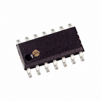
PIC16F630-I/SL Microchip Technology, PIC16F630-I/SL Datasheet - Page 21

PIC16F630-I/SL
Manufacturer Part Number
PIC16F630-I/SL
Description
IC MCU FLASH 1KX14 EEPROM 14SOIC
Manufacturer
Microchip Technology
Series
PIC® 16Fr
Datasheets
1.PIC16F616T-ISL.pdf
(8 pages)
2.PIC12F629T-ISN.pdf
(24 pages)
3.PIC16F630-ISL.pdf
(132 pages)
4.PIC16F630-ISL.pdf
(2 pages)
5.PIC16F630-ISL.pdf
(10 pages)
6.PIC16F676-EP.pdf
(132 pages)
7.PIC16F676-ISL.pdf
(130 pages)
Specifications of PIC16F630-I/SL
Program Memory Type
FLASH
Program Memory Size
1.75KB (1K x 14)
Package / Case
14-SOIC (3.9mm Width), 14-SOL
Core Processor
PIC
Core Size
8-Bit
Speed
20MHz
Peripherals
Brown-out Detect/Reset, POR, WDT
Number Of I /o
12
Eeprom Size
128 x 8
Ram Size
64 x 8
Voltage - Supply (vcc/vdd)
2 V ~ 5.5 V
Oscillator Type
Internal
Operating Temperature
-40°C ~ 85°C
Processor Series
PIC16F
Core
PIC
Data Bus Width
8 bit
Data Ram Size
64 B
Interface Type
RS- 232/USB
Maximum Clock Frequency
20 MHz
Number Of Programmable I/os
12
Number Of Timers
2
Operating Supply Voltage
2 V to 5.5 V
Maximum Operating Temperature
+ 85 C
Mounting Style
SMD/SMT
3rd Party Development Tools
52715-96, 52716-328, 52717-734
Development Tools By Supplier
PG164130, DV164035, DV244005, DV164005, PG164120, ICE2000, DM163014, DM164120-4
Minimum Operating Temperature
- 40 C
Package
14SOIC N
Device Core
PIC
Family Name
PIC16
Maximum Speed
20 MHz
Lead Free Status / RoHS Status
Lead free / RoHS Compliant
Data Converters
-
Connectivity
-
Lead Free Status / Rohs Status
Lead free / RoHS Compliant
Available stocks
Company
Part Number
Manufacturer
Quantity
Price
Company:
Part Number:
PIC16F630-I/SL
Manufacturer:
TriQuint
Quantity:
1 200
Company:
Part Number:
PIC16F630-I/SL
Manufacturer:
MICROCHI
Quantity:
1 743
Part Number:
PIC16F630-I/SL
Manufacturer:
MICROCHIP/微芯
Quantity:
20 000
3.0
There are as many as twelve general purpose I/O pins
available. Depending on which peripherals are
enabled, some or all of the pins may not be available as
general purpose I/O. In general, when a peripheral is
enabled, the associated pin may not be used as a
general purpose I/O pin.
3.1
PORTA is an 6-bit wide, bidirectional port. The corre-
sponding data direction register is TRISA. Setting a
TRISA bit (= 1) will make the corresponding PORTA pin
an input (i.e., put the corresponding output driver in a
High-Impedance mode). Clearing a TRISA bit (= 0) will
make the corresponding PORTA pin an output (i.e., put
the contents of the output latch on the selected pin).
The exception is RA3, which is input only and its TRIS
bit will always read as ‘1’. Example 3-1 shows how to
initialize PORTA.
Reading the PORTA register reads the status of the
pins, whereas writing to it will write to the PORT latch.
All write operations are read-modify-write operations.
Therefore, a write to a port implies that the port pins are
read, this value is modified and then written to the
PORT data latch. RA3 reads ‘0’ when MCLREN = 1.
The TRISA register controls the direction of the
PORTA pins, even when they are being used as analog
inputs. The user must ensure the bits in the TRISA
REGISTER 3-1:
2010 Microchip Technology Inc.
Note:
PORTS A AND C
PORTA and the TRISA Registers
bit 7-6:
bit 5-0:
Additional information on I/O ports may be
found in the PIC
Manual, (DS33023)
PORTA — PORTA REGISTER (ADDRESS: 05h)
Unimplemented: Read as ‘0’
PORTA<5:0>: PORTA I/O pin bits
1 = Port pin is >V
0 = Port pin is <V
bit 7
Legend:
R = Readable bit
- n = Value at POR
U-0
—
®
Mid-Range Reference
U-0
—
IH
IL
R/W-x
RA5
W = Writable bit
‘1’ = Bit is set
R/W-x
RA4
register are maintained set when using them as analog
inputs. I/O pins configured as analog input always read
‘0’.
EXAMPLE 3-1:
3.2
Every PORTA pin on the PIC16F630/676 has an
interrupt-on-change option and every PORTA pin,
except RA3, has a weak pull-up option. The next two
sections describe these functions.
3.2.1
Each of the PORTA pins, except RA3, has an individu-
ally configurable weak internal pull-up. Control bits
WPUAx enable or disable each pull-up. Refer to
Register 3-3. Each weak pull-up is automatically turned
off when the port pin is configured as an output. The
pull-ups are disabled on a Power-on Reset by the
RAPU bit (OPTION<7>).
BCF
CLRF
MOVLW
MOVWF
BSF
CLRF
MOVLW
MOVWF
BCF
Note:
Additional Pin Functions
U = Unimplemented bit, read as ‘0’
‘0’ = Bit is cleared
STATUS,RP0
PORTA
05h
CMCON
STATUS,RP0
ANSEL
0Ch
TRISA
STATUS,RP0
R/W-x
The ANSEL (91h) and CMCON (19h)
registers must be initialized to configure an
analog channel as a digital input. Pins
configured as analog inputs will read ‘0’.
The ANSEL register is defined for the
PIC16F676.
RA3
WEAK PULL-UP
PIC16F630/676
INITIALIZING PORTA
R/W-x
RA2
;Bank 0
;Init PORTA
;Set RA<2:0> to
;digital I/O
;Bank 1
;digital I/O
;Set RA<3:2> as inputs
;and set RA<5:4,1:0>
;as outputs
;Bank 0
x = Bit is unknown
R/W-x
RA1
DS40039F-page 21
R/W-x
RA0
bit 0


