PIC16F677-I/P Microchip Technology, PIC16F677-I/P Datasheet - Page 201
PIC16F677-I/P
Manufacturer Part Number
PIC16F677-I/P
Description
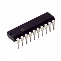
IC PIC MCU FLASH 2KX14 20DIP
Manufacturer
Microchip Technology
Series
PIC® 16Fr
Datasheets
1.PIC16F616T-ISL.pdf
(8 pages)
2.PIC16F690DM-PCTLHS.pdf
(306 pages)
3.PIC16F677-IP.pdf
(2 pages)
4.PIC16F677-IP.pdf
(16 pages)
5.PIC16F677-ISO.pdf
(294 pages)
Specifications of PIC16F677-I/P
Program Memory Type
FLASH
Program Memory Size
3.5KB (2K x 14)
Package / Case
20-DIP (0.300", 7.62mm)
Mfg Application Notes
Intro to Capacitive Sensing Appl Notes Layout and Physical Design Appl Note
Core Processor
PIC
Core Size
8-Bit
Speed
20MHz
Connectivity
I²C, SPI
Peripherals
Brown-out Detect/Reset, POR, WDT
Number Of I /o
18
Eeprom Size
256 x 8
Ram Size
128 x 8
Voltage - Supply (vcc/vdd)
2 V ~ 5.5 V
Data Converters
A/D 12x10b
Oscillator Type
Internal
Operating Temperature
-40°C ~ 85°C
Processor Series
PIC16F
Core
PIC
Data Bus Width
8 bit
Data Ram Size
128 B
Interface Type
SSP
Maximum Clock Frequency
20 MHz
Number Of Programmable I/os
17
Number Of Timers
2
Operating Supply Voltage
2 V to 5.5 V
Maximum Operating Temperature
+ 85 C
Mounting Style
Through Hole
3rd Party Development Tools
52715-96, 52716-328, 52717-734
Development Tools By Supplier
PG164130, DV164035, DV244005, DV164005, PG164120, ICE2000, DM163014, DM164120-4
Minimum Operating Temperature
- 40 C
On-chip Adc
12-ch x 10-bit
Lead Free Status / RoHS Status
Lead free / RoHS Compliant
For Use With
AC162061 - HEADER INTRFC MPLAB ICD2 20PINACICE0203 - MPLABICE 20P 300 MIL ADAPTER
Lead Free Status / Rohs Status
Lead free / RoHS Compliant
Available stocks
Company
Part Number
Manufacturer
Quantity
Price
Company:

Part Number:
PIC16F677-I/P
Manufacturer:
MICROCHIP
Quantity:
2 000


REGISTER 14-1:
© 2008 Microchip Technology Inc.
bit 13
bit 6
Legend:
R = Readable bit
-n = Value at POR
bit 13-12
bit 11
bit 10
bit 9-8
bit 7
bit 6
bit 5
bit 4
bit 3
bit 2-0
Note
Reserved
CP
1:
2:
3:
4:
(3)
Enabling Brown-out Reset does not automatically enable Power-up Timer.
The entire data EEPROM will be erased when the code protection is turned off.
The entire program memory will be erased when the code protection is turned off.
When MCLR is asserted in INTOSC or RC mode, the internal clock oscillator is disabled.
Reserved: Reserved bits. Do Not Use.
FCMEN: Fail-Safe Clock Monitor Enabled bit
1 = Fail-Safe Clock Monitor is enabled
0 = Fail-Safe Clock Monitor is disabled
IESO: Internal External Switchover bit
1 = Internal External Switchover mode is enabled
0 = Internal External Switchover mode is disabled
BOREN<1:0>: Brown-out Reset Selection bits
11 = BOR enabled
10 = BOR enabled during operation and disabled in Sleep
01 = BOR controlled by SBOREN bit of the PCON register
00 = BOR disabled
CPD: Data Code Protection bit
1 = Data memory code protection is disabled
0 = Data memory code protection is enabled
CP: Code Protection bit
1 = Program memory code protection is disabled
0 = Program memory code protection is enabled
MCLRE: MCLR Pin Function Select bit
1 = MCLR pin function is MCLR
0 = MCLR pin function is digital input, MCLR internally tied to V
PWRTE: Power-up Timer Enable bit
1 = PWRT disabled
0 = PWRT enabled
WDTE: Watchdog Timer Enable bit
1 = WDT enabled
0 = WDT disabled
FOSC<2:0>: Oscillator Selection bits
111 =
110 =
101 =
100 =
011 =
010 =
001 =
000 =
MCLRE
Reserved
CONFIG: CONFIGURATION WORD REGISTER
RC oscillator: CLKOUT function on RA4/OSC2/CLKOUT pin, RC on RA5/OSC1/CLKIN
RCIO oscillator: I/O function on RA4/OSC2/CLKOUT pin, RC on RA5/OSC1/CLKIN
INTOSC oscillator: CLKOUT function on RA4/OSC2/CLKOUT pin,
I/O function on RA5/OSC1/CLKIN
INTOSCIO oscillator: I/O function on RA4/OSC2/CLKOUT pin,
I/O function on RA5/OSC1/CLKIN
EC: I/O function on RA4/OSC2/CLKOUT pin, CLKIN on RA5/OSC1/CLKIN
HS oscillator: High-speed crystal/resonator on RA4/OSC2/CLKOUT and RA5/OSC1/CLKIN
XT oscillator: Crystal/resonator on RA4/OSC2/CLKOUT and RA5/OSC1/CLKIN
LP oscillator: Low-power crystal on RA4/OSC2/CLKOUT and RA5/OSC1/CLKIN
(4)
W = Writable bit
‘1’ = Bit is set
(2)
PIC16F631/677/685/687/689/690
FCMEN
PWRTE
(2)
(4)
(1)
WDTE
IESO
DD
P = Programmable’
‘0’ = Bit is cleared
BOREN1
FOSC2
(1)
BOREN0
FOSC1
(1)
DS41262E-page 199
U = Unimplemented
bit, read as ‘0’
x = Bit is unknown
FOSC0
CPD
bit 7
bit 0
(2
Related parts for PIC16F677-I/P
Image
Part Number
Description
Manufacturer
Datasheet
Request
R

Part Number:
Description:
3.5KB Flash, 128B RAM, 18 I/O, CLC, CWG, DDS, 10-bit ADC 20 QFN 4x4mm TUBE
Manufacturer:
Microchip Technology
Datasheet:

Part Number:
Description:
3.5KB Flash, 128B RAM, 18 I/O, CLC, CWG, DDS, 10-bit ADC 20 PDIP .300in TUBE
Manufacturer:
Microchip Technology
Datasheet:

Part Number:
Description:
3.5KB Flash, 128B RAM, 18 I/O, CLC, CWG, DDS, 10-bit ADC 20 SOIC .300in TUBE
Manufacturer:
Microchip Technology
Datasheet:

Part Number:
Description:
3.5KB Flash, 128B RAM, 18 I/O, CLC, CWG, DDS, 10-bit ADC 20 SSOP .209in TUBE
Manufacturer:
Microchip Technology
Datasheet:
Part Number:
Description:
3.5KB Flash, 128B RAM, 18 I/O, CLC, CWG, DDS, 10-bit ADC 20 QFN 4x4mm TUBE
Manufacturer:
Microchip Technology
Datasheet:
Part Number:
Description:
3.5KB Flash, 128B RAM, 18 I/O, CLC, CWG, DDS, 10-bit ADC 20 PDIP .300in TUBE
Manufacturer:
Microchip Technology
Datasheet:
Part Number:
Description:
3.5KB Flash, 128B RAM, 18 I/O, CLC, CWG, DDS, 10-bit ADC 20 SOIC .300in TUBE
Manufacturer:
Microchip Technology
Datasheet:
Part Number:
Description:
3.5KB Flash, 128B RAM, 18 I/O, CLC, CWG, DDS, 10-bit ADC 20 SSOP .209in TUBE
Manufacturer:
Microchip Technology
Datasheet:
Part Number:
Description:
3.5KB Flash, 128B RAM, 18 I/O, CLC, CWG, DDS, 10-bit ADC 20 QFN 4x4mm T/R
Manufacturer:
Microchip Technology
Datasheet:
Part Number:
Description:
3.5KB Flash, 128B RAM, 18 I/O, CLC, CWG, DDS, 10-bit ADC 20 SOIC .300in T/R
Manufacturer:
Microchip Technology
Datasheet:
Part Number:
Description:
3.5KB Flash, 128B RAM, 18 I/O, CLC, CWG, DDS, 10-bit ADC 20 SSOP .209in T/R
Manufacturer:
Microchip Technology
Datasheet:
Part Number:
Description:
3.5KB Flash, 128B RAM, 18 I/O, CLC, CWG, DDS, 10-bit ADC 20 QFN 4x4mm TUBE
Manufacturer:
Microchip Technology
Datasheet:
Part Number:
Description:
3.5KB Flash, 128B RAM, 18 I/O, CLC, CWG, DDS, 10-bit ADC 20 PDIP .300in TUBE
Manufacturer:
Microchip Technology
Datasheet:
Part Number:
Description:
3.5KB Flash, 128B RAM, 18 I/O, CLC, CWG, DDS, 10-bit ADC 20 SOIC .300in TUBE
Manufacturer:
Microchip Technology
Datasheet:
Part Number:
Description:
3.5KB Flash, 128B RAM, 18 I/O, CLC, CWG, DDS, 10-bit ADC 20 SSOP .209in TUBE
Manufacturer:
Microchip Technology
Datasheet: