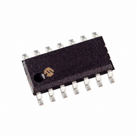
PIC16F526-I/SL Microchip Technology, PIC16F526-I/SL Datasheet - Page 23

PIC16F526-I/SL
Manufacturer Part Number
PIC16F526-I/SL
Description
IC PIC MCU FLASH 1KX12 14SOIC
Manufacturer
Microchip Technology
Series
PIC® 16Fr
Datasheets
1.PIC16F526-ISL.pdf
(122 pages)
2.PIC16F526-ISL.pdf
(22 pages)
3.PIC16F526-IP.pdf
(104 pages)
Specifications of PIC16F526-I/SL
Core Size
8-Bit
Program Memory Size
1.5KB (1K x 12)
Core Processor
PIC
Speed
20MHz
Peripherals
POR, WDT
Number Of I /o
11
Program Memory Type
FLASH
Ram Size
67 x 8
Voltage - Supply (vcc/vdd)
2 V ~ 5.5 V
Data Converters
A/D 3x8b
Oscillator Type
Internal
Operating Temperature
-40°C ~ 85°C
Package / Case
14-SOIC (3.9mm Width), 14-SOL
Controller Family/series
PIC16F
No. Of I/o's
12
Eeprom Memory Size
64Byte
Ram Memory Size
67Byte
Cpu Speed
20MHz
No. Of Timers
1
Processor Series
PIC16F
Core
PIC
Data Bus Width
8 bit
Data Ram Size
67 B
Maximum Clock Frequency
20 MHz
Number Of Programmable I/os
12
Number Of Timers
1
Maximum Operating Temperature
+ 85 C
Mounting Style
SMD/SMT
3rd Party Development Tools
52715-96, 52716-328, 52717-734
Development Tools By Supplier
PG164130, DV164035, DV244005, DV164005, PG164120, ICE2000
Minimum Operating Temperature
- 40 C
On-chip Adc
8 bit, 3 Channel
A/d Bit Size
8 bit
A/d Channels Available
3
Height
1.25 mm
Length
8.65 mm
Supply Voltage (max)
5.5 V
Supply Voltage (min)
2 V
Width
3.9 mm
Lead Free Status / RoHS Status
Lead free / RoHS Compliant
For Use With
ICE2000 - EMULATOR MPLAB-ICE 2000 POD
Eeprom Size
-
Connectivity
-
Lead Free Status / Rohs Status
Details
Available stocks
Company
Part Number
Manufacturer
Quantity
Price
Part Number:
PIC16F526-I/SL
Manufacturer:
MICROCHIP/微芯
Quantity:
20 000
5.0
The data memory is the Flash data memory block,
which attaches to the user Flash program memory. It is
located at addresses 0x400-0x43F, as shown in Figure
5-1.
This Flash data memory block consists of 8 rows and
has self-write capability of up to 64 bytes. This memory
block is not directly mapped in the register file space.
Instead, it is indirectly addressed through the Special
Function Registers. There are three SFRs used to read
and write this memory:
• EEDATA (Register 5-1)
• EEADR (Register 5-2)
• EECON (Register 5-3)
REGISTER 5-1:
REGISTER 5-2:
© 2007 Microchip Technology Inc.
bit 7
Legend:
R = Readable bit
-n = Value at POR
bit 7-0
bit 7
Legend:
R = Readable bit
-n = Value at POR
bit 7-6
bit 5-0
EEDATA7
R/W-x
U-0
—
FLASH DATA MEMORY
EEDATA<7:0>: 8-bits of data to be read from/written to data Flash
Unimplemented: Do not use
EEADR<5:0>: 6-bits of data to be read from/written to data Flash
EEDATA6
R/W-x
U-0
—
EEDATA: FLASH DATA REGISTER
EEADR: FLASH ADDRESS REGISTER
W = Writable bit
‘1’ = Bit is set
W = Writable bit
‘1’ = Bit is set
EEDATA5
EEADR5
R/W-x
R/W-x
EEDATA4
EEADR4
R/W-x
R/W-x
Preliminary
U = Unimplemented bit, read as ‘0’
U = Unimplemented bit, read as ‘0’
‘0’ = Bit is cleared
‘0’ = Bit is cleared
EEDATA3
EEADR3
R/W-x
R/W-x
EEDATA holds the 8-bit data for read/write, and
EEADR holds the address of the EEDATA location
being accessed. The effective program counter is
EEADR + 400h with only the lower 8 bits of each word
being readable or writable.
• EEADR = 00h, PC = 400h
• EEADR = 01h, PC = 401h
The Flash data memory allows byte read and write, and
during the operations of read and write cycles, the CPU
stalls.
The timing for all self-writes and erases is controlled by
the internal timing block of the program memory (see
Section 14.0
Table 14-11). The write/erase voltages are generated
by an on-chip charge pump rated to operate over the
voltage range of the device for byte or word operations.
When the device is code-protected, the CPU may
continue to read and write the Flash data memory and
read the program memory. When code-protected, the
device programmer can no longer access data or
program memory.
EEDATA2
EEADR2
R/W-x
R/W-x
“Electrical
x = Bit is unknown
x = Bit is unknown
PIC16F526
EEDATA1
EEADR1
R/W-x
R/W-x
Characteristics”,
DS41326A-page 21
EEDATA0
EEADR0
R/W-x
R/W-x
bit 0
bit 0


