1SMB75CAT3 ON Semiconductor, 1SMB75CAT3 Datasheet
1SMB75CAT3
Specifications of 1SMB75CAT3
Available stocks


Related parts for 1SMB75CAT3

1SMB75CAT3 Summary of contents
Page 1
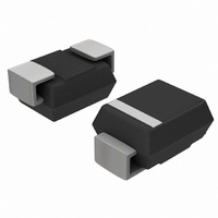
... They have excellent clamping capability, high surge capability, low zener impedance and fast response time. The SMB series is supplied in ON Semiconductor’s exclusive, cost-effective, highly reliable Surmetict package and is ideally suited for use in communication systems, automotive, numerical controls, process controls, medical equipment, business machines, power supplies and many other industrial/consumer applications ...
Page 2
... Recommended Operating Conditions is not implied. Extended exposure to stresses above the Recommended Operating Conditions may affect device reliability 1000 ms, non−repetitive 2. 1″ square copper pad, FR−4 board 3. FR−4 board, using ON Semiconductor minimum recommended footprint, as shown in 403A case outline dimensions spec *Please see 1SMB5.0AT3 to 1SMB170AT3 for Unidirectional devices ELECTRICAL CHARACTERISTICS (T = 25° ...
Page 3
... MZC 1SMB54CAT3, G NEC 1SMB58CAT3, G NGC 1SMB60CAT3, G NKC 1SMB64CAT3, G NMC 1SMB75CAT3, G NRC 4. A transient suppressor is normally selected according to the working peak reverse voltage (V the DC or continuous peak operating voltage level measured at pulse test current ambient temperature of 25° Surge current waveform per Figure 2 and derate per Figure 3 of the General Data − 600 Watt at the beginning of this group. ...
Page 4
... Figure 4. Typical Junction Capacitance vs. Bias TYPICAL PROTECTION CIRCUIT Z in LOAD V http://onsemi.com 4 PULSE WIDTH ( DEFINED P AS THAT POINT WHERE THE PEAK CURRENT DECAYS TO 50 HALF VALUE - TIME (ms) Figure 2. Pulse Waveform 1SMB10CAT3G 1SMB18CAT3G 1SMB48CAT3G 1SMB75CAT3G 10 BIAS VOLTAGE (V) Voltage L 5 100 ...
Page 5
RESPONSE TIME In most applications, the transient suppressor device is placed in parallel with the equipment or component to be protected. In this situation, there is a time delay associated with the capacitance of the device and an overshoot condition ...
Page 6
TIME DELAY DUE TO CAPACITIVE EFFECT D Figure 5. 1 0.7 0.5 0.3 0.2 0.1 0.07 0.05 0.03 0.02 0.01 The entire series has Underwriters Laboratory Recognition for the classification of protectors (QVGQ2) ...
Page 7
... *For additional information on our Pb−Free strategy and soldering details, please download the ON Semiconductor Soldering and Mounting Techniques Reference Manual, SOLDERRM/D. SURMETIC is a trademark of Semiconductor Components Industries, LLC. ON Semiconductor and are registered trademarks of Semiconductor Components Industries, LLC (SCILLC). SCILLC reserves the right to make changes without further notice to any products herein ...