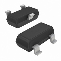
NUP1105LT1G ON Semiconductor, NUP1105LT1G Datasheet - Page 2

NUP1105LT1G
Manufacturer Part Number
NUP1105LT1G
Description
IC BUS PROTECTOR CAN/LIN SOT-23
Manufacturer
ON Semiconductor
Datasheet
1.NUP1105LT1G.pdf
(6 pages)
Specifications of NUP1105LT1G
Voltage - Reverse Standoff (typ)
24V
Voltage - Breakdown
25.7V
Power (watts)
350W
Polarization
Bidirectional
Mounting Type
Surface Mount
Package / Case
SOT-23-3, TO-236-3, Micro3™, SSD3, SST3
Polarity
Bidirectional
Channels
1 Channel
Clamping Voltage
44 V
Operating Voltage
24 V (Min)
Breakdown Voltage
25.7 V
Termination Style
SMD/SMT
Peak Surge Current
8 A
Peak Pulse Power Dissipation
350 W
Capacitance
60 pF
Maximum Operating Temperature
+ 150 C
Minimum Operating Temperature
- 55 C
Dimensions
1.3 mm W x 2.9 mm L
Reverse Stand-off Voltage Vrwm
24V
Breakdown Voltage Range
25.7V To 28.4V
Clamping Voltage Vc Max
40V
Peak Pulse Current Ippm
8A
Diode Case Style
SOT-23
No. Of Pins
3
Termination Type
SMD
Rohs Compliant
Yes
Lead Free Status / RoHS Status
Lead free / RoHS Compliant
Other names
NUP1105LT1G
NUP1105LT1GOSTR
NUP1105LT1GOSTR
Available stocks
Company
Part Number
Manufacturer
Quantity
Price
Company:
Part Number:
NUP1105LT1G
Manufacturer:
ON
Quantity:
45 000
Company:
Part Number:
NUP1105LT1G
Manufacturer:
ON
Quantity:
30 000
Company:
Part Number:
NUP1105LT1G
Manufacturer:
ON
Quantity:
30 000
Part Number:
NUP1105LT1G
Manufacturer:
ON/安森美
Quantity:
20 000
2. TVS devices are normally selected according to the working peak reverse voltage (V
3. V
4. Pulse waveform per Figure 1.
MAXIMUM RATINGS
Maximum ratings are those values beyond which device damage can occur. Maximum ratings applied to the device are individual stress limit
values (not normal operating conditions) and are not valid simultaneously. If these limits are exceeded, device functional operation is not im-
plied, damage may occur and reliability may be affected.
1. Nonrepetitive current pulse per Figure 1.
ELECTRICAL CHARACTERISTICS
Symbol
Symbol
V
ESD
PPK
V
or continuous peak operating voltage level.
RWM
V
V
I
CJ
T
T
T
I
PP
BR
R
BR
C
C
J
J
L
is measured at pulse test current I
Peak Power Dissipation
8 x 20 ms Double Exponential Waveform (Note 1)
Operating Junction Temperature Range
Storage Temperature Range
Lead Solder Temperature (10 s)
Human Body model (HBM)
Machine Model (MM)
IEC 61000−4−2 Specification (Contact)
Reverse Working Voltage
Breakdown Voltage
Reverse Leakage Current
Clamping Voltage
Clamping Voltage
Maximum Peak Pulse Current
Capacitance
Parameter
(T
J
= 25°C, unless otherwise specified)
T
.
(T
J
Rating
(Note 2)
I
V
I
I
8 x 20 ms Waveform (Note 4)
V
V
= 25°C, unless otherwise specified)
T
PP
PP
RWM
R
R
= 1 mA (Note 3)
= 0 V, f = 1 MHz (Anode to GND)
= 0 V, f = 1 MHz (Anode to Anode)
= 5 A (8 x 20 ms Waveform) (Note 4)
= 8 A (8 x 20 ms Waveform) (Note 4)
= 24 V
Test Conditions
http://onsemi.com
NUP1105L
2
RWM
), which should be equal or greater than the DC
25.7
Min
24
−55 to 150
−55 to 150
Value
350
260
400
Typ
16
30
15
Max
28.4
100
8.0
40
44
60
30
Unit
Unit
nA
°C
°C
°C
kV
kV
pF
W
V
V
V
V
V
A


