SMDA15CE3/TR7 Microsemi Commercial Components Group, SMDA15CE3/TR7 Datasheet - Page 2
SMDA15CE3/TR7
Manufacturer Part Number
SMDA15CE3/TR7
Description
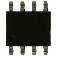
TVS ARRAY BIDIR 15.0 VWM SO-8
Manufacturer
Microsemi Commercial Components Group
Series
TVS Array™r
Datasheet
1.SMDA15CE3TR7.pdf
(2 pages)
Specifications of SMDA15CE3/TR7
Voltage - Reverse Standoff (typ)
15V
Voltage - Breakdown
16.7V
Power (watts)
300W
Polarization
4 Channel Array - Bidirectional
Mounting Type
Surface Mount
Package / Case
8-SOIC (3.9mm Width)
Lead Free Status / RoHS Status
Lead free / RoHS Compliant
Other names
SMDA15C
SMDA15CMSTR
SMDA15CTR13
SMDA15CMSTR
SMDA15CTR13


Copyright © 2005
11-11-2005 REV R
Symbol
V
V
V
I
C
WM
BR
D
C
10.0
0.01
DIM
1.0
0.1
A
B
C
D
G
K
P
F
J
L
8700 E. Thomas Rd. PO Box 1390, Scottsdale, AZ 85252 USA, (480) 941-6300, Fax: (480) 947-1503
Stand Off Voltage: Maximum dc voltage that can be applied over the operating temperature range.
Minimum Breakdown Voltage: Minimum voltage the device will exhibit at a specified current
Clamping Voltage: Maximum clamping voltage across the TVS device when subjected to a given current at a
pulse time of 20 µs.
Standby Current: Leakage current at V
Capacitance: Capacitance of the TVS as defined @ 0 volts at a frequency of 1 MHz and stated in picofarads.
V
0.188
0.150
0.053
0.011
0.016
0.006
0.005
0.189
0.228
Peak Pulse Power vs Pulse Time
MIN
WM
0.050 BSC
INCHES
must be selected to be equal or be greater than the operating voltage of the line to be protected.
S C O T T S D A L E D I V I S I O N
OUTLINE
0.197
0.158
0.069
0.021
0.050
0.010
0.008
0.206
0.244
MAX
Figure 1
MILLIMETERS
3.381
4.77
1.35
0.28
0.41
0.15
0.10
4.80
5.79
MIN
1.27 BSC
MAX
5.00
4.01
1.75
0.53
1.27
0.25
0.20
5.23
6.19
OUTLINE AND SCHEMATIC
SYMBOLS & DEFINITIONS
Scottsdale Division
Microsemi
WM.
GRAPHS
1
2
3
4
Definition
Unidirectional
and SMDB03 thru SMDB24C, e3
SMDA03 thru SMDA24C, e3
PAD LAYOUT
4 LINE TVSarray ™
SCHEMATIC
8
7
6
5
Pulse Wave Form
1
2
3
4
Figure 2
Bidirectional
8
7
6
5
Page 2
Related parts for SMDA15CE3/TR7
Image
Part Number
Description
Manufacturer
Datasheet
Request
R

Part Number:
Description:
TVS ARRAY BIDIR 15.0 VWM SO-8
Manufacturer:
Microsemi Commercial Components Group
Datasheet:
Part Number:
Description:
TVS ARRAY BIDIR 15.0 VWM SO-8
Manufacturer:
Microsemi Commercial Components Group
Datasheet:
Part Number:
Description:
TVS ARRAY BIDIR 5.0 VWM SO-16
Manufacturer:
Microsemi Commercial Components Group
Datasheet:
Part Number:
Description:
TVS ARRAY BIDIR 12.0 VWM SO-16
Manufacturer:
Microsemi Commercial Components Group
Datasheet:
Part Number:
Description:
TVS ARRAY BIDIR 15.0 VWM SO-16
Manufacturer:
Microsemi Commercial Components Group
Datasheet:
Part Number:
Description:
DIODE ARRAY 14-SOIC
Manufacturer:
Microsemi Commercial Components Group
Datasheet:

Part Number:
Description:
DIODE ZENER 12V 5W T-18
Manufacturer:
Microsemi Commercial Components Group
Datasheet:

Part Number:
Description:
DIODE ZENER 11V 1.5W SMA
Manufacturer:
Microsemi Commercial Components Group
Datasheet:
Part Number:
Description:
DIODE ZENER 5.6V 5W SMB
Manufacturer:
Microsemi Commercial Components Group
Datasheet:
Part Number:
Description:
DIODE ZENER 4.7V 5W T-18
Manufacturer:
Microsemi Commercial Components Group
Datasheet:
Part Number:
Description:
DIODE ZENER 5.1V 5W T-18
Manufacturer:
Microsemi Commercial Components Group
Datasheet:
Part Number:
Description:
DIODE ZENER 5.6V 5W T-18
Manufacturer:
Microsemi Commercial Components Group
Datasheet:
Part Number:
Description:
DIODE ZENER 6.2V 5W T-18
Manufacturer:
Microsemi Commercial Components Group
Datasheet:
Part Number:
Description:
DIODE ZENER 6.8V 5W T-18
Manufacturer:
Microsemi Commercial Components Group
Datasheet:
Part Number:
Description:
DIODE ZENER 7.5V 5W T-18
Manufacturer:
Microsemi Commercial Components Group
Datasheet: