VESD05A4A-HS4-GS08 Vishay, VESD05A4A-HS4-GS08 Datasheet
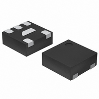
VESD05A4A-HS4-GS08
Specifications of VESD05A4A-HS4-GS08


Related parts for VESD05A4A-HS4-GS08

VESD05A4A-HS4-GS08 Summary of contents
Page 1
... Pin plating NiPdAu (e4) no whisker growth • Compliant to RoHS directive 2002/95/EC and in accordance to WEEE 2002/96/EC Marking (example only) XY 20932 Ordering Information Device name VESD05A4A-HS4 VESD05A4A-HS4-GS08 Package Data Package Type Device name name code VESD05A4A-HS4 LLP1010- Please see document “Vishay Material Category Policy”: ...
Page 2
... Storage temperature BiAs-Mode (4-line Bidirectional Asymmetrical protection mode) With the VESD05A4A-HS4 signal- or data-lines (L1 to L4) can be protected against voltage transients. With pin 2 and 6 connected to ground and pin and 5 connected to a signal- or data-line which has to be protected. As long as the voltage level on the data- or signal-line is between 0 V (ground level) and the specified Maximum Reverse Working Voltage (V isolation to the ground line ...
Page 3
... Forward clamping voltage Capacitance higher surge current or peak pulse current (I VESD05A4A-HS4 can also be used in parallel in order to "multiply" the performance. If two diodes are switched in parallel you get • double surge power = double peak pulse current ( • half of the line inductance = reduced clamping voltage • ...
Page 4
... L3) and pin 3 to ground. Pin 2 and 6 must not be connected! Positive and negative voltage transients will be clamped in the same way. The clamping current from one data line through the VESD05A4A-HS4 to the ground passes one diode in forward direction and the other one in reverse direction. The Clamping Voltage (V plus the forward voltage of the other diode plus the voltage drop at the series impedances (resistances and inductances) of the protection device ...
Page 5
... Figure 4. Typical Forward Current 0.01 20890 Figure 5. Typical Reverse Voltage 20891 Figure 6. Typical Peak Clamping Voltage V R ESDprotection@vishay.com VESD05A4A-HS4 Vishay Semiconductors 0.6 0.7 0.8 0 (V) F vs. Forward Voltage 100 1000 10000 I (µA) R vs. R Reverse Current I R positive surge V Measured C acc ...
Page 6
... VESD05A4A-HS4 Vishay Semiconductors 12 10 positive surge 8 6 Measured V 4 acc. IEC 61000-4-5 (8/20 µs - wave form) 2 BiAs-mode negative surge - 20892 I (A) PP Figure 7. Typical Peak Clamping VoltageV Peak Pulse Current acc. IEC 61000-4 contact discharge (ns) 20893 Figure 8. Typical Clamping Performance Contact Discharge (acc. IEC 61000-4-2) 40 acc ...
Page 7
... Rev. 1.4, 02-Mar-10 LLP1010-6L 0.22 (0.009) exp. DAP 0.25 (0.010) 0.15 (0.006) 1.05 (0.041) 0.95 (0.037) Foot print recommendation: 0.3 (0.012) 0.22 (0.009) ESDprotection@vishay.com VESD05A4A-HS4 Vishay Semiconductors 0.35 (0.014) Solder resist mask Solder pad Soldermask opening ± 0.03 measured middle of the package www.vishay.com 7 ...
Page 8
... Vishay product could result in personal injury or death. Customers using or selling Vishay products not expressly indicated for use in such applications their own risk and agree to fully indemnify and hold Vishay and its distributors harmless from and against any and all claims, liabilities, expenses and damages arising or resulting in connection with such use or sale, including attorneys fees, even if such claim alleges that Vishay or its distributor was negligent regarding the design or manufacture of the part ...