C1210C221JGGACTU Kemet, C1210C221JGGACTU Datasheet - Page 9
C1210C221JGGACTU
Manufacturer Part Number
C1210C221JGGACTU
Description
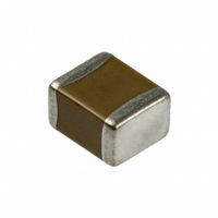
CAP CER 220PF 2000V C0G 1210
Manufacturer
Kemet
Datasheet
1.C1210C221JGGACTU.pdf
(10 pages)
Specifications of C1210C221JGGACTU
Capacitance
220pF
Voltage - Rated
2000V (2kV)
Tolerance
±5%
Temperature Coefficient
C0G, NP0
Mounting Type
Surface Mount, MLCC
Operating Temperature
-55°C ~ 125°C
Features
High Voltage
Applications
General Purpose
Package / Case
1210 (3225 Metric)
Size / Dimension
0.138" L x 0.102" W (3.50mm x 2.60mm)
Thickness
1.70mm
Capacitor Application
High Voltage
Dielectric Characteristic
C0G / NP0
Capacitance Tolerance
± 5%
Voltage Rating
2000V
Capacitor Case Style
1210
No. Of Pins
2
Capacitor
RoHS Compliant
Capacitor Mounting
SMD
Operating Temperature Range
-55°C To
Rohs Compliant
Yes
Lead Free Status / RoHS Status
Lead free / RoHS Compliant
Ratings
-
Lead Spacing
-
Other names
C1210C221JGGAC
C1210C221JGGAC7800
C1210C221JGGAC7800
Available stocks
Company
Part Number
Manufacturer
Quantity
Price


96
Sketch A:
Bending Radius
See Note 2
Table 1
Punched Carrier (Paper Tape) Configuration (Ceramic Chips Only):
12mm
8mm
Tape
Size
and
©KEMET Electronics Corporation, P.O. Box 5928, Greenville, S.C. 29606, (864) 963-6300
Note:
1. A 0 , B 0 and T determined by the maximum dimensions to the ends of the terminals extending from the
body and/or the body dimensions of the component. The clearance between the ends of the terminals or
body of the component to the sides and depth of the cavity (A 0 , B 0 and T) must be within 0.05mm (.002)
minimum and 0.50mm (.020) maximum. The clearance allowed must also prevent rotation of the component
within the cavity of not more than 20 degrees (see sketches A and B).
2. Tape with components shall pass around radius "R" without damage.
3. KEMET nominal thicknesses are: 0402 = 0.6mm and all others 0.95mm minimum.
Double
12mm
12mm
8mm
Pitch
8mm
Pitch
Tape
Size
Bottom
1/2
Cover
Tape
+0.004, -0.0)
+0.10, -0.0
(.059
D
1.5
Section 3.3 (d)
(0.157
(0.157
(0.315
See Require-
0
(.079 .004)
2.0
4.0
4.0
8.0
ments
T
T
P
1
1
0.10
0.10
0.10
0.10
(.069 0.004)
Cover
.004)
.004)
.004)
Tape
1.75 0.10
Top
User Direction of Feed
R
(Min.)
CERAMIC CHIP CAPACITORS
Constant Dimensions - Millimeters (Inches)
E
Variable Dimensions - Millimeters (Inches)
Table 1: 8 & 12mm Punched Tape
Table 1: 8 & 12mm Punched Tape
(.138
(.217
3.5
5.5
(
(
Metric Dimensions Will Govern)
Metric Dimensions Will Govern)
F
20
0.05
0.05
(.157
.002)
.002)
4.0
Packaging Information
P
D
0
0.10
0.004)
0
(.472
(.315
Cross Sectional View
12.0
8.0
Max. Component
A
Rotation - Front
0
Max. Cavity Size
(.079
Sketch B:
W
See Note 1
2.0
.012)
0.012)
Table 1
0.3
0.3
B
P
0
1
P
2
0.05
0.002)
P
0
P
See Note 1
2
(.004)
Max.
Table 1
0.10
A
T
Center lines
of cavity
1
0
B
0
10 pitches cumulative
tolerance on tape
(.030)
0.2 ( 0.008)
0.75
Min.
G
1
Component Rotation - Top View
1.1mm (.043)
Max. for Paper
Base Tape and
1.6mm (.063)
Max. for Non-
Paper Base
Compositions.
See Note 3.
(.030)
0.75
Min.
G
2
G
T
E
2
20
Sketch C:
F
See Note 2
25 (.984)
W
Maximum
component rotation.
Table 1
R Min.
Typical
component
center line
Related parts for C1210C221JGGACTU
Image
Part Number
Description
Manufacturer
Datasheet
Request
R

Part Number:
Description:
CAP, KEMET #F601BL105K250C
Manufacturer:
Kemet
Datasheet:
Part Number:
Description:
Manufacturer:
Kemet
Datasheet:
Part Number:
Description:
Manufacturer:
Kemet
Datasheet: