DS32ELX0421SQ/NOPB National Semiconductor, DS32ELX0421SQ/NOPB Datasheet
DS32ELX0421SQ/NOPB
Specifications of DS32ELX0421SQ/NOPB


Related parts for DS32ELX0421SQ/NOPB

DS32ELX0421SQ/NOPB Summary of contents
Page 1
... Displays: LED walls, Commercial ■ Video Transport ■ Communication Systems ■ Test and Measurement ■ Industrial Bus Typical Application © 2010 National Semiconductor Corporation DS32EL0421, DS32ELX0421 Features ■ 5-bit DDR LVDS parallel data interface ■ Programmable transmit de-emphasis ■ Configurable output levels (V ■ ...
Page 2
Connection Diagrams www.national.com 2 30032102 ...
Page 3
3 30032103 www.national.com ...
Page 4
Pin Descriptions Pin Name Pin Number I/O, Type Description Power, Ground and Analog Reference VDD33 VDD VDD25 7, 15, 18, 25, I, VDD 35 VDDPLL 28 I, VDD VOD_CTRL 14 Analog LF_CP 27 Analog LF_REF 26 Analog ...
Page 5
Pin Name Pin Number I/O, Type Description Other GPIO0 3 I/O, LVCMOS GPIO1 4 I/O, LVCMOS GPIO2 11 I/O, LVCMOS 12, 13, Misc. 19, 20, 21, 22, 23, 24 13, 21, Misc. 22, 23, ...
Page 6
... Absolute Maximum Ratings If Military/Aerospace specified devices are required, please contact the National Semiconductor Sales Office/ Distributors for availability and specifications. Supply Voltage (3. DD33 Supply Voltage (2. DD25 LVCMOS Input Voltage LVCMOS Output Voltage LVDS Input Voltage (IN+, IN-) CML Output Voltage Junction Temperature ...
Page 7
LVCMOS Electrical Specifications Over recommended operating supply and temperature ranges unless otherwise specified. Applies to GPIO0, GPIO1, GPIO2, RESET, LOCK, RS, and DC_BAL. (Note Symbol Parameter V High Level Input Voltage IH V Low Level Input Voltage IL V High ...
Page 8
LVDS Electrical Specifications Over recommended operating supply and temperature ranges unless otherwise specified. Symbol Parameter V Differential Input High Threshold TH V Differential Input Low Threshold TL V LVDS Input Common Mode Voltage LVCM V LVDS Input Loss of Signal ...
Page 9
Symbol Parameter t Serializer Bit Width BIT t Serializer Propagation Delay – Latency SD t Serializer Output Deterministic Jitter JIND t Serializer Output Random Jitter JINR t Peak-to-peak Serializer Output Jitter JINT λ Jitter Transfer Function -3 dB Bandwidth TXBW ...
Page 10
Timing Diagrams FIGURE 3. Serializer (LVDS Interface) Setup/Hold and High/Low Times www.national.com FIGURE 1. SMBus timing parameters FIGURE 2. Serializer Input Clock Transition Time 10 30032106 30032111 30032110 ...
Page 11
FIGURE 4. LVDS Input Clock Delay FIGURE 5. Propagation Delay Timing Diagram FIGURE 6. 5-Bit Parallel LVDS Inputs Mapped to CML Output 11 30032113 30032112 30032104 www.national.com ...
Page 12
Functional Description POWER SUPPLIES The DS32EL0421 and DS32ELX0421 have several power supply pins, at 2.5V as well as 3.3V important that these pins all be connected and properly bypassed. Bypassing should consist of parallel 4.7μF and 0.1μF capacitors ...
Page 13
SCRAMBLER and NRZI Encoder The CDR of the DS32EL0124 and the DS32ELX0124 expect a transition density of 20% for a period of 200 μs. If the scram- bler and NRZI encoder are enabled, the raw or DC-balanced serialized data is ...
Page 14
This feature is used to pass link status information between the 2 devices. When Remote Sense is enabled the serializer will send a training pattern to the de- serializer to establish lock and lane alignment. If DC-Balance ...
Page 15
SMBus INTERFACE The System Management Bus interface is compatible to SM- Bus 2.0 physical layer specification. The use of the Chip Select signal is required. Holding the SMB_CS pin HIGH en- ables the SMBus port, allowing access to the configuration ...
Page 16
FIGURE 8. SMBus Configuration 1 FIGURE 9. SMBus Configuration 2 FIGURE 10. SMBus Daisy Chained CS Configuration 16 30032107 30032108 30032109 ...
Page 17
PROPAGATION DELAY Once the serializer is locked, the amount of time it takes for a bit to travel into the device through the DDR LVDS inputs and out through the CML serial output is defined to be the propagation delay. ...
Page 18
Applications Information GPIO PINS The GPIO pins can be useful tools when debugging or eval- uating the system. For specific GPIO configurations and func- tions refer to registers and 6 in the device register map. GPIO ...
Page 19
FIGURE 12. Typical Interface Circuit 19 30032105 www.national.com ...
Page 20
Typical Performance Characteristics The eye diagrams shown below illustrate the typical perfor- mace of the DS32ELX0421/DS32EL0421 configured with RS = 0,DC_B = 0, for the conditions listed below each figure. CML Serial Differential Output 1.25 Gbps CML Serial Singled Ended ...
Page 21
Register Map The register information for the serializer is shown in the table below. Some registers have been omitted or marked as re- Addr Name Bits (Hex) 00 Device ID 7:1 SMBus Address 0 Reserved 01 Reset 7:5 Reserved 4 ...
Page 22
Addr Name Bits (Hex 7 Out 7 07–1F Reserved 20 De-Emphasis 7:3 2 1:0 21 Device Config 1:0 22 Device Config 7:5 Override ...
Page 23
Addr Name Bits (Hex) 26 Power Down 7 Channel Reset 6 Clock Powerdown 5 LVDS Clock enable 4 TxIN4 Enable 3 TxIN3 Enable 2 TxIN2 Enable 1 TxIN1 Enable 0 TxIN0 Enable 27 Event Disable 7:5 Reserved 4 PLL Lock ...
Page 24
Addr Name Bits (Hex) 2B Event Config Event Count 7:0 2D Reserved 2E Analog Driver Config 7 ...
Page 25
Addr Name Bits (Hex) 69 Output Amplitude 7:3 Reserved Adjust 2:0 Amplitude Adjust R/W Field R/W Default 0 011’b 000: Level 7 001: Level 8 (Highest output) 010: Level 5 011: Level 6 (Normal output) 100: Level 4 101: Level ...
Page 26
Register Recipes Many features of the serializer contained within the SMBus registers require multiple writes to configure and enable. This methodology was implemented to prevent accidental register writes from causing undesired device behavior. Several recipes for common features are listed ...
Page 27
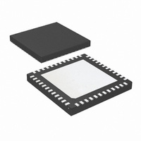
Physical Dimensions inches (millimeters) unless otherwise noted (See AN-1187 for PCB Design and Assembly Recommendations) 48–Lead LLP Plastic Quad Package NS Package Number SQA48A 27 www.national.com ...
Page 28
... For more National Semiconductor product information and proven design tools, visit the following Web sites at: www.national.com Products Amplifiers www.national.com/amplifiers Audio www.national.com/audio Clock and Timing www.national.com/timing Data Converters www.national.com/adc Interface www.national.com/interface LVDS www.national.com/lvds Power Management www.national.com/power Switching Regulators www.national.com/switchers LDOs www.national.com/ldo LED Lighting www ...