ADIS16255/PCBZ Analog Devices Inc, ADIS16255/PCBZ Datasheet - Page 15
ADIS16255/PCBZ
Manufacturer Part Number
ADIS16255/PCBZ
Description
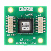
BOARD EVAL FOR ADIS16255
Manufacturer
Analog Devices Inc
Series
iMEMS®, iSensor™r
Specifications of ADIS16255/PCBZ
Sensor Type
Gyroscope, 1 Axis (Yaw Rate)
Sensing Range
±80°/sec, ±160°/sec, ±320°/sec
Interface
SPI Serial
Sensitivity
0.018°/sec/LSB
Voltage - Supply
4.75 V ~ 5.25 V
Embedded
No
Utilized Ic / Part
ADIS16255
For Use With
ADISUSBZ - KIT EVAL ADIS W/SOFTWARE USBADISEVALZ - KIT PC EVALUATION W/SOFTWARE
Lead Free Status / RoHS Status
Lead free / RoHS Compliant
Available stocks
Company
Part Number
Manufacturer
Quantity
Price

Part Number:
ADIS16255/PCBZ
Manufacturer:
ADI/亚德诺
Quantity:
20 000


OPERATIONAL CONTROL
Internal Sample Rate
The internal sample rate defines how often data output
variables are updated, independent of the rate at which they
are read out on the SPI port. The SMPL_PRD register controls
the ADIS16250/ADIS16255 internal sample rate and has two
parts: a selectable time base and a multiplier. The sample
period can be calculated using the following equation:
where:
T
T
N
The default value is the maximum 256 samples per second,
and the contents of this register are nonvolatile.
Table 15. SMPL_PRD Register Definition
Address
0x37, 0x36
Table 16. SMPL_PRD Bit Descriptions
Bit
15:8
7
6:0
The following is an example calculation of the sample period
for the ADIS16250/ADIS16255:
The sample rate setting has a direct impact on the SPI data
rate capability. For sample rates of 64 SPS and above, the SPI
SCLK can run at a rate up to 2.5 MHz. For sample rates
below 64 SPS, the SPI SCLK can run at a rate up to 1 MHz.
The sample rate setting also affects the power dissipation.
When the sample rate is set below 64 SPS, the power dissipation
reduces by a factor of 60%. The two different modes of
operation offer a system-level trade-off between performance
(sample rate, serial transfer rate) and power dissipation.
Power Management
In addition to offering two different performance modes for
power optimization, the ADIS16250/ADIS16255 offer a
programmable shutdown period. Writing the appropriate
sleep time to the SLP_CNT register shuts the device down
for the specified time. The following example provides an
illustration of this relationship:
S
B
S
is the sample period.
is the time base.
is the increment setting.
T
If SMPL_PRD = 0x0007, B7…B0 = 00000111
B7 = 0 → T
B6…B0 = 000000111 → N
T
f
B7 … B0 = 00000110
Sleep period = 3 sec
S
S
S
= 1∕T
Description
Not used
Time base, 0 = 1.953 ms, 1 = 60.54 ms
Multiplier
= T
= T
B
B
S
× (N
× (N
= 64 SPS
B
Default
0x0001
= 1.953 ms
S
S
+ 1)
+ 1) = 1.953 ms × (7 + 1) = 15.624 ms
S
= 7
Format
N/A
Access
R/W
Rev. D | Page 15 of 20
After completing the sleep period, the ADIS16250/ADIS16255 return
to normal operation. If measurements are required before sleep
period completion, the ADIS16250/ADIS16255 can be awakened
by putting the CS line in a zero logic state. Otherwise, the CS line
must be kept high to maintain sleep mode.
Table 17. SLP_CNT Register Definition
Address
0x3B, 0x3A
1
Table 18. SLP_CNT Bit Descriptions
Bit
15:8
7:0
Analog Bandwidth
The analog bandwidth of the ADIS16250/ADIS16255 is 50 Hz.
This bandwidth can be reduced by placing an external capacitor
across the RATE and FILT pins. In this case, the analog bandwidth
can be calculated using the following equation:
where:
R
C
Digital Filtering
The ADIS16250/ADIS16255 GYRO_OUT signal path has a nominal
analog bandwidth of 50 Hz. The ADIS16250 provides a Bartlett
Window FIR filter for additional noise reduction on all of the output
data registers. The SENS/AVG register stores the number of taps in
this filter in seven power-of-two step sizes (that is, 2
32, 64, and 128). Filter setup requires one simple step: write the
appropriate M factor to the assigned bits in the SENS/AVG register.
The bit assignments are listed in Table 20. The following equation
offers a frequency response relationship for this filter:
Scale is the weight of each LSB.
OUT
OUT
f
= 45.22 kΩ.
is the external capacitance.
H
OUT
B
–100
–120
–140
–160
(
= 1/(2 × π × R
–20
–40
–60
–80
f
0.001
0
)
Figure 23. Bartlett Window FIR Frequency Response
=
Description
Not used
Data bits
Scale
0.5 sec
H
A
2
(
1
f
)
⇒
OUT
N = 128
Default
0x0000
H
0.01
× (C
A
FREQUENCY (f/fs)
(
f
ADIS16250/ADIS16255
OUT
)
N = 16
=
+ 0.068 μF))
Format
Binary
sin(
N
×
π
N = 4
sin(
×
0.1
N
π
×
×
Access
R/W
f
f
M
×
×
= 1, 2, 4, 16,
t
t
N = 2
S
S
)
)
1
Related parts for ADIS16255/PCBZ
Image
Part Number
Description
Manufacturer
Datasheet
Request
R

Part Number:
Description:
±1.7g Dual-Axis IMEMS Accelerometer Evaluation Board
Manufacturer:
Analog Devices Inc
Datasheet:

Part Number:
Description:
Inertial Sensor Evaluation System
Manufacturer:
Analog Devices Inc
Datasheet:
Part Number:
Description:
Manufacturer:
Analog Devices Inc
Datasheet:
Part Number:
Description:
Manufacturer:
Analog Devices Inc
Datasheet:
Part Number:
Description:
Manufacturer:
Analog Devices Inc
Datasheet:
Part Number:
Description:
Manufacturer:
Analog Devices Inc
Datasheet:
Part Number:
Description:
Manufacturer:
Analog Devices Inc
Datasheet:
Part Number:
Description:
Manufacturer:
Analog Devices Inc
Datasheet:
Part Number:
Description:
Manufacturer:
Analog Devices Inc
Datasheet:
Part Number:
Description:
Manufacturer:
Analog Devices Inc
Datasheet:
Part Number:
Description:
Manufacturer:
Analog Devices Inc
Datasheet:
Part Number:
Description:
Manufacturer:
Analog Devices Inc
Datasheet:
Part Number:
Description:
Manufacturer:
Analog Devices Inc
Datasheet: