EVAL-AD7663CB Analog Devices Inc, EVAL-AD7663CB Datasheet - Page 4
EVAL-AD7663CB
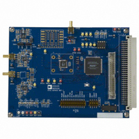
Manufacturer Part Number
EVAL-AD7663CB
Description
BOARD EVAL FOR AD7663
Manufacturer
Analog Devices Inc
Series
PulSAR®r
Datasheet
1.AD7663ASTZ.pdf
(24 pages)
Specifications of EVAL-AD7663CB
Number Of Adc's
1
Number Of Bits
16
Sampling Rate (per Second)
250k
Data Interface
Serial, Parallel
Inputs Per Adc
1 Single Ended
Input Range
±4 REF
Power (typ) @ Conditions
35mW @ 250kSPS
Voltage Supply Source
Analog and Digital
Operating Temperature
-40°C ~ 85°C
Utilized Ic / Part
AD7663
Lead Free Status / RoHS Status
Contains lead / RoHS non-compliant


TIMING SPECIFICATIONS
Parameter
Refer to Figures 17 and 18 (Master Serial Interface Modes)
Refer to Figures 19 and 21 (Slave Serial Interface Modes)
NOTES
1
2
Specifications subject to change without notice.
AD7663
DIVSCLK[1]
DIVSCLK[0]
SYNC to SCLK First Edge Delay Minimum
Internal SCLK Period Minimum
Internal SCLK Period Maximum
Internal SCLK HIGH Minimum
Internal SCLK LOW Minimum
SDOUT Valid Setup Time Minimum
SDOUT Valid Hold Time Minimum
SCLK Last Edge to SYNC Delay Minimum
BUSY HIGH Width Maximum
In serial interface modes, the SYNC, SCLK, and SDOUT timings are defined with a maximum load C
In Serial Master Read during Convert Mode. See Table II for Master Read after Convert Mode.
CS HIGH to SYNC HI-Z
CS HIGH to Internal SCLK HI-Z
CS HIGH to SDOUT HI-Z
BUSY HIGH in Master Serial Read after Convert
CNVST LOW to SYNC Asserted Delay
SYNC Deasserted to BUSY LOW Delay
External SCLK Setup Time
External SCLK Active Edge to SDOUT Delay
SDIN Setup Time
SDIN Hold Time
External SCLK Period
External SCLK HIGH
External SCLK LOW
(Master Serial Read after Convert)
Figure 1. Load Circuit for Digital Interface Timing
*IN SERIAL INTERFACE MODES, THE SYNC, SCLK, AND
TO OUTPUT
SDOUT TIMINGS ARE DEFINED WITH A MAXIMUM LOAD
C
L
OF 10pF; OTHERWISE, THE LOAD IS 60pF MAXIMUM.
PIN
C
60pF*
L
500 A
1.6mA
Table II. Serial Clock Timings in Master Read after Convert
I
I
OH
OL
(continued)
1.4V
t
t
t
t
t
t
t
t
t
18
19
19
20
21
22
23
24
28
1
–4–
t
t
Symbol
t
t
t
t
t
t
t
t
t
t
t
25
26
27
28
29
30
31
32
33
34
35
36
37
0
0
4
25
40
15
9.5
4.5
2
3
2
Figure 2. Voltage Reference Levels for Timing
Min
5
3
5
5
25
10
10
0
1
20
50
70
25
24
22
4
60
2.5
t
L
DELAY
0.8V
of 10 pF; otherwise, the load is 60 pF maximum.
2V
0.8V
Typ
See Table II
1.25
25
1
0
20
100
140
50
49
22
30
140
3.5
2V
1
1
20
200
280
100
99
22
90
300
5.75
Max
10
10
10
16
t
DELAY
2V
0.8V
Unit
ns
ns
ns
ns
ns
ns
ns
ns
µs
REV. B
Unit
ns
ns
ns
µs
µs
ns
ns
ns
ns
ns
ns
ns
ns
Related parts for EVAL-AD7663CB
Image
Part Number
Description
Manufacturer
Datasheet
Request
R

Part Number:
Description:
ENERCHIP CC EVAL KIT
Manufacturer:
Cymbet Corporation
Datasheet:

Part Number:
Description:
BOARD EVAL FOR AD976
Manufacturer:
Analog Devices Inc
Datasheet:

Part Number:
Description:
BOARD EVAL FOR ADXL345
Manufacturer:
Analog Devices Inc
Datasheet:

Part Number:
Description:
ENERCHIP CC SEH EVAL KIT
Manufacturer:
Cymbet Corporation
Datasheet:

Part Number:
Description:
ENERCHIP EP ENERGY HARVEST EVAL
Manufacturer:
Cymbet Corporation
Datasheet:

Part Number:
Description:
EVAL BOARD FOR TW6864-LB2-GR
Manufacturer:
Intersil
Datasheet:
Part Number:
Description:
EVAL BOARD FOR TW8816-LB3-GR
Manufacturer:
Intersil
Datasheet:
Part Number:
Description:
EVAL BOARD FOR TW8817-TA3-GRS
Manufacturer:
Intersil
Datasheet:

Part Number:
Description:
EVALUATION MODULE FOR ADUM4160
Manufacturer:
Analog Devices Inc
Datasheet:

Part Number:
Description:
BOARD EVALUATION ADCMP581BCP
Manufacturer:
Analog Devices Inc
Datasheet:
Part Number:
Description:
BOARD EVALUATION ADM1041
Manufacturer:
Analog Devices Inc
Datasheet:

Part Number:
Description:
EVAL BOARD FOR STM32F107VCT
Manufacturer:
STMicroelectronics
Datasheet:
Part Number:
Description:
BOARD EVAL FOR AD1954
Manufacturer:
Analog Devices Inc
Datasheet:
Part Number:
Description:
BOARD EVAL FOR AD1955
Manufacturer:
Analog Devices Inc
Datasheet:

Part Number:
Description:
BOARD EVAL FOR AD7655
Manufacturer:
Analog Devices Inc
Datasheet: