AD8369-EVAL Analog Devices Inc, AD8369-EVAL Datasheet
AD8369-EVAL
Specifications of AD8369-EVAL


Related parts for AD8369-EVAL


AD8369-EVAL Summary of contents
Page 1
... Digital control pins can be driven with standard CMOS logic levels. The AD8369 may be powered on or off by a logic level applied to the PWUP pin. For a logic high, the chip powers up rapidly to its nominal quiescent current 25ºC. When low, the total dissipation drops to less than a few milliwatts ...
Page 2
... AD8369–SPECIFICATIONS Parameter Conditions OVERALL FUNCTION Frequency Range 3 dB Bandwidth GAIN CONTROL INTERFACE Voltage Gain Span Maximum Gain All bits high ( Minimum Gain All bits low ( Gain Step Size Gain Step Accuracy Over entire gain range, with respect step Gain Step Response Time ...
Page 3
... V p-p OPHI OPLO – p-p OPHI OPLO – p-p composite OPHI OPLO – p-p OPHI OPLO – p-p OPHI OPLO –3– AD8369 Min Typ Max 40.5 ± 0.1 7.0 +19.5 +19.5 –69 –68 – 40.0 ± 0.10 7.0 +17 +17 –64 – ...
Page 4
... AD8369 SPECIFICATIONS (Continued) Parameter Conditions Frequency = 380 MHz Voltage Gain Within ± 20 MHz of 380 MHz Gain Flatness Noise Figure Output IP3 f1 = 379.55 MHz 380.45 MHz IMD f1 = 379.55 MHz 380.45 MHz OPHI Harmonic Distortion Second-Order, V Third-Order, V For ± deviation from linear gain P1dB Specifications subject to change without notice ...
Page 5
... ESD (electrostatic discharge) sensitive device. Electrostatic charges as high as 4000 V readily accumulate on the human body and test equipment and can discharge without detection. Although the AD8369 features proprietary ESD protection circuitry, permanent damage may occur on devices subjected to high energy electrostatic discharges. Therefore, proper ESD precautions are recommended to avoid performance degradation or loss of functionality ...
Page 6
... Power-Up Pin. Connect PWUP to VPOS to power up the device. Connect PWUP to COMM to power-down. 15 COMM Device Common. Connect to a low impedance ground. 16 INHI Balanced Differential Input. Internally biased, should be ac-coupled. PIN CONFIGURATION INLO 1 16 INHI COMM 2 15 COMM AD8369 BIT0 3 14 PWUP TOP VIEW BIT1 4 13 VPOS (Not To Scale) BIT2 5 12 SENB BIT3 ...
Page 7
... FREQUENCY – MHz TPC 2. Maximum Gain vs. Frequency by R Supply Voltage GAIN CODE TPC 3. Output IP3 vs. Gain Code at 70 MHz 200 REV. 0 Typical Performance Characteristics–AD8369 200 TPC 4. Gain vs. Frequency by Gain Code 5V 200 1000 and TPC 5. Gain vs. Frequency by Gain Code, R ...
Page 8
... AD8369 –63 –64 –65 –66 –67 –68 –69 – GAIN CODE TPC 7. Two-Tone, IMD vs. Gain Code at 70 MHz – p- OPHI OPLO 100 150 200 250 FREQUENCY – MHz TPC 8. Harmonic Distortion at V OPHI = Maximum Gain Frequency GAIN CODE TPC 9. Noise Figure vs. Gain Code at 70 MHz, V ...
Page 9
... Maximum Gain, V Appendix for Definition) 0.75 250 0.50 200 OPHI 0.25 150 OPLO 0 100 1000 10 TPC 18. Equivalent Output Resistance and Capacitance vs. Frequency at Maximum Gain –9– AD8369 –1 –2 –3 –4 –5 –6 –7 100 1000 FREQUENCY – MHz = 100 1000 FREQUENCY – ...
Page 10
... AD8369 90 120 150 GAIN CODE 15 750MHz 180 GAIN CODES 0, 1, AND 9 210 240 270 TPC 19. Differential Input Reflection Coefficient Differential, Selected Gain Codes AVERAGE OF 128 SAMPLES DIFFERENTIAL OUTPUT 250mV/VERTICAL DIVISION ZERO BIT 0 2V/VERTICAL DIVISION GND TIME – 20ns/DIV TPC 20. Gain Step Time Domain Response Step, ...
Page 11
... + –2 –2 –7 1000 = 5 V, TPC 30. Output P1dB vs. Frequency by Temperature –11– AD8369 GAIN ERROR AND 85 C WITH RESPECT DATA BASED ON 45 PARTS FROM TWO BATCH LOTS. 10 100 FREQUENCY – MHz = 200 W , Maximum Gain = GAIN ERROR AND 85 C WITH RESPECT DATA BASED PARTS FROM TWO BATCH LOTS ...
Page 12
... AD8369 3.06 3.08 3.10 GAIN STEP SIZE – dB/CODE TPC 31. Distribution of Gain Step Size, 70 MHz –74 –73 –72 –71 –70 –69 –68 –67 –66 –65 –64 –63 –62 IMD – dBc TPC 32. Distribution of IMD , 70 MHz – p-p Composite, V OPHI OPLO Maximum Gain ...
Page 13
... Input and Output Interfaces The dc working points of the differential input and output inter- faces of the AD8369 are internally biased. The inputs INHI and INLO are biased to a diode drop below V positive supply) to meet isolation and headroom constraints, while the outputs OPHI and OPLO are centered on the supply ...
Page 14
... See TPCs 3 and 9. Offset Control Loop The AD8369 uses a control loop to null offsets at the input. If left uncorrected, these offsets, in conjunction with the gain of the AD8369, would reduce the available voltage swing at the output ...
Page 15
... Reducing Gain Sensitivity to Input and Output Impedance Variation The lot-to-lot variations in gain mentioned previously can, in principle, be eliminated by adjustments to the source and load. Define a term as a function of the input and output resistances of the AD8369 and the source and load resistances presented to it ...
Page 16
... Figure 6 shows HD3 = –80dBc SNR = 51dB an FFT of the AD8369 delivering a single tone at –1 dBFS (that is p-p) at the input of the ADC with an HD2 of –83 dBc and HD3 of –80 dBc. Figure 7 shows that the two-tone, third-order intermodulation distortion level is – ...
Page 17
... REV Figure 8. Cross-Sectional View Board The AD8369 contains both digital and analog sections. Care should be taken to ensure that the digital and analog sections are adequately isolated on the PC board. The use of separate ground planes for each section connected at only one point via a ferrite bead inductor will ensure that the digital pulses do not adversely affect the analog section of the AD8369 ...
Page 18
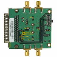
... The evaluation board is connected via a cable to the parallel port of the computer. By simply adjusting the slider bar in the control software, the gain code is automatically updated to the AD8369. On some older PCs, it may be necessary to use 5 kW pull-up resistors to VPOS on DATA, CLOCK, and LATCH depending upon the capabilities of the port transceiver necessary to set SW3 on the evaluation board to “ ...
Page 19
... SW2 Device Enable: When in the PWDN position, the PWUP pin will be connected to ground and the AD8369 will be disabled. The device is enabled when the switch is in the PWUP position, connecting the PWUP pin to VPOS. SW3, R5 Serial/Parallel Selection. The device will respond to serial control inputs from connector P1 when the switch is in the SER position ...
Page 20
... CMRR, and s-parameter information. Except for the s-parameter informa- tion, T-attenuator pads were used to match the 50 W impedance of the ports of this instrument to the AD8369. An Anritsu MS4623B “Scorpion” Vector Network Analyzer was used to obtain nonlinear measurements IMD through matching baluns and attenuator networks ...
Page 21
... FILT CMDC OPHI AD8369 COMM BIT0 BIT1 BIT2 BIT3 DENB OPLO CONTROL INTERFACE ANRITSU MS4623B VNA SOURCE RECEIVER OUTPUT INPUT Figure 14. Vector Network Analyzer Setup ( –21– AD8369 10nF 10 9 MINI-CIRCUITS TC4-1W OPLO 7 8 10nF 604 10nF MINI-CIRCUITS TC4-1W 4120 237 604 10nF ...
Page 22
... BIT2 BIT3 DENB OPLO Figure 16. Gain Step Response Setup –22– 0.1 F 1nF 100nF PWUP VPOS SENB FILT CMDC OPHI AD8369 BIT1 BIT2 BIT3 DENB OPLO 100nF V S 604 10nF AGILENT INFINIUM MINI-CIRCUITS 4120 237 TC4-1W 604 10nF TEK P6248 DIFF R L ...
Page 23
... BIT2 BIT3 DENB OPLO Figure 18. Overdrive Response Setup –23– TEK TDS 5104 DSO V S 5.0V 100nF 9 TEK P6248 DIFF 1000 PROBE OPLO 8 100nF 604 10nF 9 AGILENT INFINIUM 4120 237 MINI-CIRCUITS TC4-1W 8 604 10nF AD8369 TEK 1103 PROBE POWER SUPPLY DSO ...
Page 24
... AD8369 16-Lead Thin Shrink Small Outline Package [TSSOP] 4.50 4.40 4.30 PIN 1 0.15 0.05 OUTLINE DIMENSIONS (RU-16) Dimensions shown in millimeters 5.10 5.00 4. 6.40 BSC 1 8 1.20 MAX 0.20 0.09 8 0.30 0.65 0 0.19 SEATING BSC PLANE COPLANARITY 0.10 COMPLIANT TO JEDEC STANDARDS MO-153AB – ...