C8051F930-TB Silicon Laboratories Inc, C8051F930-TB Datasheet
C8051F930-TB
Specifications of C8051F930-TB


Related parts for C8051F930-TB

C8051F930-TB Summary of contents
Page 1
... Notes: 1. The target board included in this kit is provided with a pre-soldered C8051F930 MCU (LQFP32 package). 2. Code developed on the C8051F930 can be easily ported to the other members of this MCU family. 3. Refer to the C8051F93x-C8051F92x data sheet for the differences between the members of this MCU family. ...
Page 2
... To complete the installation process, connect the included USB cable between the host computer and the USB connector (P3) on the C8051F930 Target Board. Windows will automatically finish the driver installation. Information windows will pop up from the taskbar to show the installation progress. ...
Page 3
... Hi-Tech SDCC The demo applications for the C8051F930 target board are written to work with the Keil and SDCC toolsets. 3.4. Keil Evaluation Toolset 3.4.1. Keil Assembler and Linker The Keil demonstration toolset assembler and linker place no restrictions on code size. ...
Page 4
... C8051F930-DK 3.5. Configuration Wizard 2 The Configuration Wizard code generation tool for all of the Silicon Laboratories devices. Code is generated through the use of dialog boxes for each of the device's peripherals. Figure 2. Configuration Wizard 2 Utility The Configuration Wizard utility helps accelerate development by automatically generating initialization source code to configure and enable the on-chip resources needed by most design projects ...
Page 5
... To create a new profile: 1. Select the profile that most closely matches the target application or choose the "Custom Profile". 2. Click Manage 3. Click Duplicate 4. Click Edit Profiles may be edited with the easy-to-use GUI (shown in Figure 4). C8051F930-DK Rev. 0.5 5 ...
Page 6
... C8051F930-DK Figure 4. Battery Life Estimator Discharge Profile Editor The Discharge Profile Editor allows the user to modify the profile name and description. The four text entry boxes on the left hand side of the form allow the user to specify the amount of time the system spends in each power mode ...
Page 7
... The primary outputs of the Battery Life Estimator are an estimated system operating time and a simulated graph of battery voltage vs. time. Additional outputs include estimated battery capacity, average current, self-discharge current, and the ability to export graph data to a comma delimited text file for plotting in an external graphing application. C8051F930-DK Rev. 0.5 7 ...
Page 8
... C8051F930-DK 3.7. Keil µVision2 and µVision3 Silicon Laboratories Drivers As an alternative to the Silicon Laboratories IDE, the µVision debug driver allows the Keil µVision2 and µVision3 IDEs to communicate with Silicon Laboratories’ on-chip debug logic. In-system Flash memory programming integrated into the driver allows for rapid updating of target code. The µVision2 and µVision3 IDEs can be used to start and stop program execution, set breakpoints, check variables, inspect and modify memory contents, and single-step through programs running on the actual target hardware. For more information, refer to the µ ...
Page 9
... Project” in the Project Window. Select Add Groups to project. Add pre-defined groups or add customized groups. Right-click on the group name and choose Add file to group. Select files to be added. Continue adding files until all project files have been added. C8051F930-DK Rev. 0.5 9 ...
Page 10
... C8051F930-DK 5.2. Building and Downloading the Program for Debugging 1. Once all source files have been added to the target build, build the project by clicking on the Build/Make Project button in the toolbar or selecting Project Note: After the project has been built the first time, the Build/Make Project command will only build the files that have been changed since the previous build ...
Page 11
... Port I/O crossbar, configuring a timer for an interrupt routine, initializing the system clock, and configuring a GPIO port pin. When compiled/assembled and linked this program flashes the green LED on the C8051F930 Target Board about five times a second using the interrupt handler with a C8051F930 timer. ...
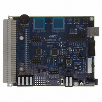
Page 12
... C8051F930-DK 7. Target Board The C8051F930 Development Kit includes a target board with a C8051F930 device pre-installed for evaluation and preliminary software development. Numerous input/output (I/O) connections are provided to facilitate prototyping using the target board. Refer to Figure 7 for the locations of the various I/O connectors. Figure 9 on page 14 shows the factory default shorting block positions ...
Page 13
... BT3 Battery Holder for 3 V Coin Cell (CR2032). BT4 Battery Holder for 1.5 V Button Cell (A76 or 357). Note: BT2 is only used in two-cell mode. BT2 (AAA) Figure 8. Bottom of C8051F930 Target Board NEG POS BT3 (CR2032) POS NEG BT4 (A76 or 357) Rev. 0.5 ...
Page 14
... C8051F930-DK 7.1. Target Board Shorting Blocks: Factory Defaults The C8051F930 target board comes from the factory with pre-installed shorting blocks on many headers. Figure 9 shows the positions of the factory default shorting blocks. R15 J16 P1.4 J15 GND PORT2 P1 PORT1 J6 VDD/DC+ H1 Pin 1 Figure 9. C8051F930 Target Board Shorting Blocks: Factory Defaults 14 P1 ...
Page 15
... V are selected when SW4 is configured to two-cell mode. 7.2.3. Coin Cell Battery When the J10/J11 three-way header is set to COIN_CELL, the C8051F930 Target Board may be powered from a single 1.5 V Alkaline (A76) or Silver Oxide (357) button cell inserted in BT4 or from a single 3 V Lithium (CR2032) coin cell inserted in BT3 ...
Page 16
... Populate C21 for capacitor mode, and populate R16 and C21 for RC mode. Refer to the C8051F93x- C8051F92x data sheet for more information on the use of external oscillators. 7.4. Port I/O Headers (J2, J3, J4, J6) Access to all Port I/O on the C8051F930 is provided through the headers J2, J3, and J4. The header J6 provides access to the ground plane for easy clipping of oscilloscope probes. 16 ...
Page 17
... Two touch sensitive (contactless) switches are provided on the target board. The operation of these switches require appropriate firmware running on the C8051F930 MCU that can sense the state of the switch. See Section 6.3. "Touch Sensitive Switch Example‚" on page 11 for details about example source code. ...
Page 18
... C8051F930-DK 7.6. Expansion I/O Connector (P1) The 96-pin Expansion I/O connector P1 provides access to all signal pins of the C8051F930 device (except the C2 debug interface signals). In addition, power supply and ground pins are included. A small through-hole prototyping area is also provided. See Table 2 for a list of pin descriptions for P1. ...
Page 19
... USB-to-UART device drivers should be installed as described in Section 3.2. "CP210x USB to UART VCP Driver Installation‚" on page 2. Table 4. Serial Interface Header (J12) Description 7.9. Analog I/O (H1) Several of the C8051F930 target device’s port pins are connected to the H1 terminal block. Refer to Table 5 for the H1 terminal block connections. Table 5. H1 Terminal Block Pin Descriptions Pin # ...
Page 20
... J2[8] and H1[2] connectors. 7.11. VREF and AGND Connector (J13, J14) The C8051F930 Target Board also features 4.7 µF capacitor in parallel with a 0.1 µF that can be connected to P0.0/VREF when using the Precision Voltage Reference. The capacitors are connected to P0.0/VREF when a shorting block is installed on J13. Using the Precision Voltage Reference is optional since 'F93x-'F92x devices have an on-chip High-Speed Voltage Reference ...
Page 21
... Alternatively, a shorting block can be placed on J17 to ensure that the multimeter does not limit current during startup. 4. Where can I find a schematic of the C8051F930 Target Board? A target board schematic can be found in the C8051F930-DK User’s Guide which is available on the Development Tools CD and is installed in the following folder (by default): C:\SiLabs\MCU\Documentation\UsersGuides 5 ...
Page 22
... C8051F930-DK 6. What can reduce active supply current? Below are some suggestions for reducing the active supply current: a. Clear all wake-up sources in the PCU0CF register. This will allow the low power oscillator to be disabled when it is not being used as the system clock. This optimization can reduce the supply current µ ...
Page 23
... The maximum VDD Ramp Time is specified at 3 ms. If the power supply ramp takes longer than reach 0.9 V, then the device may be released from reset before the supply has reached the minimum operating voltage. The slow ramp time (>3 ms) can occur when using a bench power supply that does not have an output enable switch. C8051F930-DK Rev. 0.5 23 ...
Page 24
... C8051F930-DK 9. Schematics 24 Rev. 0.5 ...
Page 25
... C8051F930-DK Rev. 0.5 25 ...
Page 26
... C8051F930-DK 26 Rev. 0.5 ...
Page 27
... N : OTES C8051F930-DK Rev. 0.5 27 ...
Page 28
... C8051F930- ONTACT NFORMATION Silicon Laboratories Inc. 400 West Cesar Chavez Austin, TX 78701 Please visit the Silicon Labs Technical Support web page: https://www.silabs.com/support/pages/contacttechnicalsupport.aspx and register to submit a technical support request. The information in this document is believed to be accurate in all respects at the time of publication but is subject to change without notice. ...