TOOLSTICK560DC Silicon Laboratories Inc, TOOLSTICK560DC Datasheet - Page 9
TOOLSTICK560DC
Manufacturer Part Number
TOOLSTICK560DC
Description
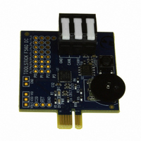
DAUGHTER CARD TOOLSTICK F560
Manufacturer
Silicon Laboratories Inc
Series
ToolStickr
Type
MCUr
Specifications of TOOLSTICK560DC
Contents
Daughter Card
Processor To Be Evaluated
C8051F55x, C8051F56x, C8051F57x
Interface Type
USB
Operating Supply Voltage
2.7 V to 3.6 V
Lead Free Status / RoHS Status
Lead free / RoHS Compliant
For Use With/related Products
C8051F55x, C8051F56x, C8051F57x
For Use With
336-1345 - TOOLSTICK BASE ADAPTER336-1182 - ADAPTER USB DEBUG FOR C8051FXXX
Lead Free Status / Rohs Status
Lead free / RoHS Compliant
Other names
336-1719


C8051F55x/56x/57x
Figure 16.1. Reset Sources ................................................................................... 136
Figure 16.2. Power-On and VDD Monitor Reset Timing ....................................... 137
Figure 17.1. Multiplexed Configuration Example ................................................... 147
Figure 17.2. EMIF Operating Modes ..................................................................... 148
Figure 17.3. Multiplexed 16-bit MOVX Timing ....................................................... 151
Figure 17.4. Multiplexed 8-bit MOVX without Bank Select Timing ........................ 152
Figure 17.5. Multiplexed 8-bit MOVX with Bank Select Timing ............................. 153
Figure 18.1. Oscillator Options .............................................................................. 155
Figure 18.2. Example Clock Multiplier Output ....................................................... 160
Figure 18.3. External 32.768 kHz Quartz Crystal Oscillator Connection Diagram 165
Figure 19.1. Port I/O Functional Block Diagram .................................................... 167
Figure 19.2. Port I/O Cell Block Diagram .............................................................. 168
Figure 19.3. Peripheral Availability on Port I/O Pins .............................................. 171
Figure 19.4. Crossbar Priority Decoder in Example Configuration ........................ 172
Figure 20.1. LIN Block Diagram ............................................................................ 191
Figure 21.1. Typical CAN Bus Configuration ......................................................... 208
Figure 21.2. CAN Controller Diagram .................................................................... 209
Figure 21.3. Four segments of a CAN Bit .............................................................. 211
Figure 22.1. SMBus Block Diagram ...................................................................... 216
Figure 22.2. Typical SMBus Configuration ............................................................ 217
Figure 22.3. SMBus Transaction ........................................................................... 218
Figure 22.4. Typical SMBus SCL Generation ........................................................ 220
Figure 22.5. Typical Master Write Sequence ........................................................ 227
Figure 22.6. Typical Master Read Sequence ........................................................ 228
Figure 22.7. Typical Slave Write Sequence .......................................................... 229
Figure 22.8. Typical Slave Read Sequence .......................................................... 230
Figure 23.1. UART0 Block Diagram ...................................................................... 233
Figure 23.2. UART0 Timing Without Parity or Extra Bit ......................................... 235
Figure 23.3. UART0 Timing With Parity ................................................................ 235
Figure 23.4. UART0 Timing With Extra Bit ............................................................ 235
Figure 23.5. Typical UART Interconnect Diagram ................................................. 236
Figure 23.6. UART Multi-Processor Mode Interconnect Diagram ......................... 237
Figure 24.1. SPI Block Diagram ............................................................................ 242
Figure 24.2. Multiple-Master Mode Connection Diagram ...................................... 245
Figure 24.3. 3-Wire Single Master and 3-Wire Single Slave Mode
Connection Diagram ......................................................................... 245
Figure 24.4. 4-Wire Single Master Mode and 4-Wire Slave Mode
Connection Diagram .......................................................................... 245
Figure 24.5. Master Mode Data/Clock Timing ....................................................... 247
Figure 24.6. Slave Mode Data/Clock Timing (CKPHA = 0) ................................... 248
Figure 24.7. Slave Mode Data/Clock Timing (CKPHA = 1) ................................... 248
Figure 24.8. SPI Master Timing (CKPHA = 0) ....................................................... 252
Figure 24.9. SPI Master Timing (CKPHA = 1) ....................................................... 252
Figure 24.10. SPI Slave Timing (CKPHA = 0) ....................................................... 253
Figure 24.11. SPI Slave Timing (CKPHA = 1) ....................................................... 253
Rev. 1.1
9
Related parts for TOOLSTICK560DC
Image
Part Number
Description
Manufacturer
Datasheet
Request
R

Part Number:
Description:
KIT TOOL EVAL SYS IN A USB STICK
Manufacturer:
Silicon Laboratories Inc
Datasheet:

Part Number:
Description:
TOOLSTICK DEBUG ADAPTER
Manufacturer:
Silicon Laboratories Inc
Datasheet:

Part Number:
Description:
TOOLSTICK BASE ADAPTER
Manufacturer:
Silicon Laboratories Inc
Datasheet:

Part Number:
Description:
TOOLSTICK DAUGHTER CARD
Manufacturer:
Silicon Laboratories Inc
Datasheet:

Part Number:
Description:
TOOLSTICK DAUGHTER CARD
Manufacturer:
Silicon Laboratories Inc
Datasheet:

Part Number:
Description:
TOOLSTICK DAUGHTER CARD
Manufacturer:
Silicon Laboratories Inc
Datasheet:

Part Number:
Description:
TOOLSTICK PROGRAMMING ADAPTER
Manufacturer:
Silicon Laboratories Inc
Datasheet:

Part Number:
Description:
TOOLSTICK DAUGHTER CARD
Manufacturer:
Silicon Laboratories Inc
Datasheet:

Part Number:
Description:
KIT STARTER TOOLSTICK
Manufacturer:
Silicon Laboratories Inc
Datasheet:

Part Number:
Description:
KIT UNIVERSITY TOOLSTICK STARTER
Manufacturer:
Silicon Laboratories Inc
Datasheet:

Part Number:
Description:
DAUGHTER CARD TOOLSTICK F330
Manufacturer:
Silicon Laboratories Inc
Datasheet:

Part Number:
Description:
CARD DAUGHTER UNIVRSTY TOOLSTICK
Manufacturer:
Silicon Laboratories Inc
Datasheet:

Part Number:
Description:
DAUGHTER CARD TOOLSTICK F582
Manufacturer:
Silicon Laboratories Inc
Datasheet:

Part Number:
Description:
DAUGHTER CARD TOOLSTICK F500
Manufacturer:
Silicon Laboratories Inc
Datasheet:

Part Number:
Description:
DAUGHTER CARD TOOLSTICK F540
Manufacturer:
Silicon Laboratories Inc
Datasheet: