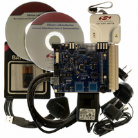
C8051F930DK Silicon Laboratories Inc, C8051F930DK Datasheet - Page 22

C8051F930DK
Manufacturer Part Number
C8051F930DK
Description
KIT DEV C8051F920,F921,F930,F931
Manufacturer
Silicon Laboratories Inc
Type
MCUr
Specifications of C8051F930DK
Contents
Target Board, Power Adapter, USB Debug Adapter, Cables, Batteries, and Software
Processor To Be Evaluated
C8051F930
Processor Series
C8051F9xx
Data Bus Width
8 bit
Interface Type
I2C, UART, SPI
Maximum Operating Temperature
+ 85 C
Minimum Operating Temperature
- 40 C
Operating Supply Voltage
0.9 V to 3.6 V
Lead Free Status / RoHS Status
Lead free / RoHS Compliant
For Use With/related Products
C8051F920, F921, F930, F931
Lead Free Status / Rohs Status
Lead free / RoHS Compliant
Other names
336-1473
Available stocks
Company
Part Number
Manufacturer
Quantity
Price
Company:
Part Number:
C8051F930DK
Manufacturer:
Silicon Labs
Quantity:
135
C8051F930-DK
6. What can I do to reduce active supply current?
7. Why does P0.7/IREF0 have a voltage of 200 mV when IREF0CN is set to 0x00?
8. I have configured a Port pin as an analog input. Why is it still shorted to ground?
9. Why does power consumption increase when an analog signal (hovering around mid-supply) is
10.Why does the dc/dc converter stop regulating when the load current exceeds 10 mA?
22
Below are some suggestions for reducing the active supply current:
When IREF0CN is set to 0x00, the current reference is completely turned off. When a shorting block is installed
on J7, the voltage at P0.7/IREF0 should be 0 V unless one of the following conditions is present:
On C8051F93x-C8051F92x devices, configuring a Port pin to analog mode (using PnMDIN) disables the digital
input path and the weak pull-up. It does not explicitly disable the output drivers.
Software can ensure that the output drivers are disabled by configuring the Port pin to open-drain output mode
(using PnMDOUT) and writing 1 to the port latch.
connected to a digital input?
This phenomenon is called the “crowbar” effect and is present in all CMOS circuitry. If the input of a CMOS
structure is not a strong 1 or 0, then both the PMOS and NMOS devices are partially turned on causing current
flow from VDD to GND.
To prevent the “crowbar” effect, ensure that pins with analog voltage levels are configured for analog I/O.
The default register settings for the dc/dc converter are optimized for low power applications requiring less than
10 mA of supply current. If the application requires additional supply current, the default values may be
overridden to provide up to 65 mW of output power.
To configure the dc/dc converter to high power mode, perform the following steps prior to enabling any high
power device:
a. Clear all wake-up sources in the PCU0CF register. This will allow the low power oscillator to be disabled
b. When operating at system clock frequencies above 10 MHz, minimize supply current by setting the
c. If the precision oscillator is not being used, turn off the precision oscillator bias by setting the OSCBIAS
a. The P0.7/IREF0 pin is not configured for analog I/O (weak pull-up enabled).
b. The P0.7/IREF0 pin is being used as CTS (a shorting block is installed on J12).
a. Set DC0CN = 0x01. This selects the high-current switches.
b. Set DC0CF = 0x04. This sets the peak inductor current limit to 500 mA.
when it is not being used as the system clock. This optimization can reduce the supply current by up to
30 µA.
BYPASS bit (FLSCL.6) to 1. If the system clock needs to decrease below 10 MHz, clear the BYPASS bit
to 0.
bit (REG0CN.4) to 0.
Rev. 0.5


