CY3684 Cypress Semiconductor Corp, CY3684 Datasheet
CY3684
Specifications of CY3684
CY3684
Q2204408


Related parts for CY3684

CY3684 Summary of contents
Page 1
EZ-USB Development Kit Manual Getting Started Rev 1.0 • Cypress Semiconductor • Personal Communications Division • • 15050 Avenue of Science • Suite 200 • San Diego, CA 92128 • ...
Page 2
... Cypress Semicon- ductor Corporation Incorporated. While reasonable precautions have been taken, Cypress Semiconductor Corporation assumes no responsibility for any errors that may appear in this document. No part of this document may be copied or reproduced in any form or by any means with- out the prior written consent of Cypress Semi- conductor Corporation ...
Page 3
Table of Contents EZ-USB Development Kit Overview . . . . . . . . . . . . . . . . . . . . . . . . . . . . . . . . . ...
Page 4
Table of Contents ...
Page 5
EZ-USB Development Kit Overview 1.1 Introduction The EZ-USB Development Kit (DVK) is the best starting point for developing an EZ-USB based product. The DVK includes everything you will need to get started: A development board, example firmware, a generic ...
Page 6
Cypress USB Console • Cypress GPIF Designer • Cypress Firmware Download Driver sample • EZ-USB Documentation and Help Files • Reference Schematics • Limited Evaluation Version of the Keil 8051 Development Tools (Compiler, Assembler, IDE, Debugger) 1.2.1 Required Tools ...
Page 7
Compatibility with Earlier EZ-USB Development Kits This EZ-USB Advanced DVK has the ability to co-exist with older EZ-USB Development Kits. This DVK uses the same basic directory structure as the older Development Kits. The only conflict with older development ...
Page 8
Windows 98 and 98SE – For PCI add-in adapters, drivers may be available from the adapter's manufacturer. However, these versions of Windows are not supported by the EZ-USB DVK. You can verify that high-speed drivers are installed and correctly ...
Page 9
Confirm Successful Installation using the Cypress USB Console Run the Cypress USB Console application and perform a "Get Device Descriptor" operation. The Console is added to the Windows Start menu by the DVK Setup program under: Start->Cypress->USB->CyConsole – EZ-USB ...
Page 10
EZ-USB Advanced Development Board 4.1 Introduction The Cypress Semiconductor EZ-USB Advanced Development Board provides a compact evalua- tion and design vehicle for the EZ-USB family. The board provides expansion and interface sig- nals on six 20-pin headers. A mating ...
Page 11
Jumpers Table 1. EZ-USB Development Board Jumpers Jumper Function Default JP1 Connects 3.3 volt power to the EZ-USB (1-2) chip. JP2 Powers the on-board 3.3 volt regulator from (1-2) USB Vbus pin JP3 Connects four GAL pins to LEDS ...
Page 12
Table 2. Typical EZ-USB external EEPROMS EEPROM Type “Small” “Large” “Small” EEPROMS are typically used to supply custom VID and PID information, allowing the EZ- USB to enumerate with a driver associated with your EZ-USB design. “Large” EEPROMS are typically ...
Page 13
Load’: SW2=ON, SW1=LARGE A “C2” load provides a method for loading the EZ-USB internal RAM with 8051 firmware before enumeration. This ‘boot load’ mechanism allows EZ-USB to enumerate as a fully cus- tom device, since the 8051 code ...
Page 14
High speed EZ-USB strobe signals (PSEN, WR#, CLKOUT, IFCLK, and RD#) are con- nected to pin 3 of each of the five connectors P1-P6, so that they may be used as the logic analyzer clock CLK1. • CLK2 is ...
Page 15
Default Alternate RESET# GPIFADR6 GPIFADR4 GPIFADR2 GPIFADR0 Default Alternate CLKOUT Default Alternate IFCLK EZ-USB Development Board Table 6. P3 Default Alternate N. 3.3V WR RDY5 RDY4 5 6 RDY3 RDY2 7 8 BKPT 9 10 N.C. ...
Page 16
Alternate WAKEUP# T2EX RxD1OUT T2OUT T0OUT 4.6 ATA Connector P8 Table 10 shows the pinout for P8, a 40-pin connector that interfaces with a standard ATA cable. Note: This is for ATA use only. SP1, 2, and 3 should be ...
Page 17
U2 -- 22v10 GAL A standard 22v10 GAL provides general purpose “glue logic” on the board. It provides the AND gate required to combine the PSEN and READ signals, adds memory map support, debug LEDs and provides three spare ...
Page 18
The third column, “Ext Flash”, allows a flash memory (or other ROM connected to the 8051 bus. This is the only configuration that starts 8051 execution from external memory (the GAL sets EA=1). Since external memory occupies ...
Page 19
U9 has the group address 0100, and is strapped to unit address 000. Therefore to read the switch values, 8051 firmware sends a control byte of 01000001 (the LSB indicates a read operation), and then reads the data byte. 4.10 ...
Page 20
These 4 jumpers must be in place Indicator The low address byte is “don’t care”. This means you can very efficiently add software test points using the following code: D5ON: mov MPAGE,#B8h movx a,@r0 ; D5OFF: ...
Page 21
Frequently Asked Questions Q1: What should I do first (after viewing the printed material from the box)? A1: Make sure the hardware works well enough to run the Tutorial. After software installation, plug in a Dev Board, and go ...
Page 22
Q10: Where can I get a summary of the registers? A10: See the register summary in the TRM. Q11: Are there any examples? A11: Yes, see the examples and readme files in the Examples folder. Q12: What's all this set ...
Page 23
Appendix A: U2 (GAL) code (file is 'FX2LP.ABL') MODULE fx2lp " Swapped dipswitch settings 00 and 10 on 4-3-98 to allow the all-switch- on default x,c,z = .X.,.C.,.Z.; "Inputs A12,A13,A14,A15 A11 nRD,nPSEN,CLKOUT mm1,mm0 "Outputs EA,nRAMOE,nRAMCE PF0,PF1,PF2,PF3 modesw = [mm1,mm0]; ...
Page 24
ELSE WHEN(modesw == 10) THEN" All program mem external { !nRAMCE = 1; !nRAMOE =!nRD # !nPSEN test_vectors ([mm1,mm0,A15,nRD,nPSEN] -> [nRAMCE, nRAMOE, EA ...
Page 25
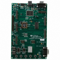
... Figure 1-2. CY3684 Assembly Development Board Layout EZ-USB Development Board Page -21 ...
Page 26
... The schematic for the CY3684 appears on the following page. Page -22 EZ-USB Development Kit Manual - Getting Started Rev 1.0 ...
Page 27
VDD Vss 24 25 VDD Vss 8 9 0805 0805 2 1 XTALOUT 11 XTALIN 12 NC3 16 NC2 15 NC1 14 VCC9 107 VCC8 100 VCC7 68 VCC6 64 VCC5 48 VCC4 43 VCC3 2 VCC2 81 VCC1 ...
Page 28
Page -24 EZ-USB Development Kit Manual - Getting Started Rev 1.0 ...