ADIS16251/PCBZ Analog Devices Inc, ADIS16251/PCBZ Datasheet - Page 10
ADIS16251/PCBZ
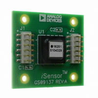
Manufacturer Part Number
ADIS16251/PCBZ
Description
BOARD EVALUATION FOR ADIS16251
Manufacturer
Analog Devices Inc
Series
iMEMS®, iSensor™r
Specifications of ADIS16251/PCBZ
Sensor Type
Gyroscope, 1 Axis
Sensing Range
±20°/sec, ±40°/sec, ±80°/sec
Interface
SPI Serial
Sensitivity
0.004°/sec/LSB
Voltage - Supply
4.75 V ~ 5.25 V
Embedded
No
Utilized Ic / Part
ADIS16251
Silicon Manufacturer
Analog Devices
Application Sub Type
Angular Rate Sensor / Gyroscope
Kit Application Type
Sensing - Motion / Vibration / Shock
Silicon Core Number
ADIS16251
Kit Contents
Board
Lead Free Status / RoHS Status
Lead free / RoHS Compliant
For Use With
ADISUSBZ - KIT EVAL ADIS W/SOFTWARE USBADISEVALZ - KIT PC EVALUATION W/SOFTWARE
Lead Free Status / RoHS Status
Lead free / RoHS Compliant


ADIS16251
THEORY OF OPERATION
OVERVIEW
The core angular rate sensor integrated into the ADIS16251
is based on the Analog Devices iMEMS technology. This sensor
operates on the principle of a resonator gyroscope. Two polysilicon
sensing structures each contain a dither frame electrostatically
driven to resonance. This provides the necessary velocity ele-
ment to produce a Coriolis force during rotation. At two of the
outer extremes of each frame (orthogonal to the dither motion)
are movable fingers placed between fixed fingers to form a capaci-
tive pickoff structure that senses Coriolis motion. The resulting
signal is fed to a series of gain and demodulation stages that
produce the electrical rate signal output.
The base sensor output signal is sampled using an ADC, and then
the digital data is fed into a proprietary digital calibration circuit.
This circuit contains calibration coefficients from the factory cali-
bration, along with user-defined calibration registers that can be
used to calibrate system-level errors.
The calibrated gyroscope data (GYRO_OUT) is made available
through output data registers along with temperature, power
supply, auxiliary ADC, and relative angle output calculations.
RELATIVE ANGLE ESTIMATE
The ANGL_OUT register offers the integration of the
GYRO_OUT data. In order for this information to be useful,
the reference angle must be known. This can be accomplished
by reading the register contents at the initial time, before starting
the monitoring, or by setting its contents to zero. This number
is reset to zero during power-up and is executed when the null
command is used as well as after a reset command. This func-
tion can be used to estimate change in an angle over a period
of time. The user is cautioned to fully understand the stability
requirements and the time period over which to use this
estimated relative angle position.
FACTORY CALIBRATION
The ADIS16251 provides a factory calibration that includes
correction for initial tolerance and power supply variation.
This calibration includes individual sensor characterization
and a custom correction coefficient calculation.
Rev. A | Page 10 of 10
AUXILIARY ADC FUNCTION
The auxiliary ADC function integrates a standard 12-bit ADC
into the ADIS16251 to digitize other system-level analog sig-
nals. The output of the ADC can be monitored through the
AUX_ADC control register, see Table 5. The ADC is a 12-bit
successive approximation converter. The output data is presented
in straight binary format with the full-scale range extending
from 0 V to 2.5 V. The 2.5 V upper limit is derived from the
on-chip precision internal reference.
Figure 15 shows the equivalent circuit of the analog input struc-
ture of the ADC. The input capacitor (C1) is typically 4 pF and
can be attributed to parasitic package capacitance. The two diodes
provide ESD protection for the analog input. Care must be taken
to ensure that the analog input signals never exceed the range
of −0.3 V to +3.5 V. This causes the diodes to become forward-
biased and to start conducting. The diodes can handle 10 mA
without causing irreversible damage. The resistor is a lumped
component that represents the on resistance of the switches.
The value of this resistance is typically 100 Ω. Capacitor C2
represents the ADC sampling capacitor and is typically 16 pF.
For ac applications, it is recommended to remove high fre-
quency components from the analog input signal by using a
low-pass filter on the analog input pin.
In applications where harmonic distortion and signal-to-noise
ratio are critical, the analog input must be driven from a low
impedance source. Large source impedances significantly affect
the ac performance of the ADC. This can necessitate the use of
an input buffer amplifier. When no input amplifier is used to drive
the analog input, the source impedance should be limited to
values lower than 1 kΩ.
Figure 15. Equivalent Analog Input Circuit,
Conversion Phase: Switch Open,
C1
Track Phase: Switch Closed
VDD
D
D
R1
C2
Related parts for ADIS16251/PCBZ
Image
Part Number
Description
Manufacturer
Datasheet
Request
R

Part Number:
Description:
±1.7g Dual-Axis IMEMS Accelerometer Evaluation Board
Manufacturer:
Analog Devices Inc
Datasheet:

Part Number:
Description:
Inertial Sensor Evaluation System
Manufacturer:
Analog Devices Inc
Datasheet:
Part Number:
Description:
Manufacturer:
Analog Devices Inc
Datasheet:
Part Number:
Description:
Manufacturer:
Analog Devices Inc
Datasheet:
Part Number:
Description:
Manufacturer:
Analog Devices Inc
Datasheet:
Part Number:
Description:
Manufacturer:
Analog Devices Inc
Datasheet:
Part Number:
Description:
Manufacturer:
Analog Devices Inc
Datasheet:
Part Number:
Description:
Manufacturer:
Analog Devices Inc
Datasheet:
Part Number:
Description:
Manufacturer:
Analog Devices Inc
Datasheet:
Part Number:
Description:
Manufacturer:
Analog Devices Inc
Datasheet:
Part Number:
Description:
Manufacturer:
Analog Devices Inc
Datasheet:
Part Number:
Description:
Manufacturer:
Analog Devices Inc
Datasheet:
Part Number:
Description:
Manufacturer:
Analog Devices Inc
Datasheet: