EVK2160A Atmel, EVK2160A Datasheet
EVK2160A
Specifications of EVK2160A
Available stocks


Related parts for EVK2160A


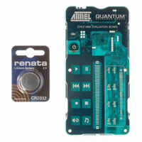
EVK2160A Summary of contents
Page 1
Features • Number of keys keys, and one slider (constructed from keys) • Number of I/O lines dedicated - configurable for input or output, 8 shared - output only), PWM control for ...
Page 2
Pinout and Pin Listing Description 2.1 Pinout Description GPIO2 GPIO3 CHANGE 2.2 Pin Listing Description Table 2-1.Pin Listing Pin AT42QT2160 ...
Page 3
Table 2-1.Pin Listing (continued) Pin Introduction The QT2160 device is a digital burst mode charge-transfer (QT) sensor designed specifically for matrix layout touch controls; ...
Page 4
Figure 3-1. 3.1 Keys and Slider The QT2160 is capable of a maximum of 16 keys. These can be located anywhere within an electrical grid of 8X and 2Y scan lines. A lesser number of enabled keys will cause any ...
Page 5
Burst Paring Keys that are disabled by setting their burst length to zero have their bursts removed from the scan sequence to save scan time and thus power. The QT2160 operates on a fixed 16 ms cycle and will ...
Page 6
Unlike other QT circuits, the Cs capacitor values on QT2160 devices have no effect on conversion gain. However, they do affect conversion time. Unused Y lines should be left open. Figure 4-1. Figure 4-2. Figure 4-3. AT42QT2160 6 VCs – ...
Page 7
Figure 4-4. Note: 4.5 Sample Resistors The sample resistors (Rs0...Rs1) are used to perform single-slope ADC conversion of the acquired charge on each Cs capacitor. These resistors directly control acquisition gain; larger values of Rs will proportionately increase signal gain. ...
Page 8
Dwell time is the duration in which charge coupled from captured on page off, causing the loss of captured charge (and hence loss of signal strength) from the keys. The dwell time is a minimum of ...
Page 9
For better surface moisture suppression, the outer perimeter of X should be as wide as possible, and there should be no ground planes near the keys. The variable “T" in this drawing represents the total thickness of all materials that ...
Page 10
Key sizes should be in the 5-7mm range when used in the slider to get the best linearity. The slider should be made up of however many of these elements are required to fit their dimensions. The slider will be ...
Page 11
LED terminals which are multiplexed or switched into a floating state and which are within or physically very near a key structure (even if on another nearby PCB) should be bypassed to either Vss or Vdd with at least a ...
Page 12
Caution: A regulator IC shared with other logic devices can result in erratic operation and is not advised. A regulator can be shared among two or more QT devices on one board. Refer to suggested regulator manufacturers. A single ceramic ...
Page 13
Spread Spectrum Acquisitions QT2160 uses spread-spectrum burst modulation. This has the effect of drastically reducing the possibility of EMI effects on the sensor keys, while simultaneously spreading RF emissions. This feature is hard-wired into the device and cannot be ...
Page 14
General Purpose Inputs/Outputs There are three dedicated GPIOs (GPIO1...3) and eight GPOs shared with X lines (X0...7). Shared GPOs are always outputs, whereas dedicated GPIOs can be set to be outputs or inputs. GPIOs set to input can be ...
Page 15
Wiring Figure 4-8. Wiring Diagram Vunreg VREG VDD Rp SDA I2C SCL VDD Rchg CHANGE I2C ADDRESS SELECT Suggested regulator manufacturers: • Toko (XC6215 series) • Seiko (S817 series) • BCDSemi (AP2121 series) Re Figure 4-8 • Section 4.3 ...
Page 16
Figure 4-9. AT42QT2160 16 Inputs/Outputs 9502A–AT42–07/08 ...
Page 17
I C-compatible Bus Operation 5.1 Interface Bus More detailed information about the www.i2C-bus.org. Devices are connected onto the Both bus lines are connected to Vdd via pull-up resistors. The bus drivers of all devices must be open-drain type. ...
Page 18
Figure 5-2. 5.3 START and STOP Conditions The host initiates and terminates a data transmission. The transmission is initiated when the host issues a START condition on the bus, and is terminated when the host issues a STOP condition. Between ...
Page 19
Figure 5-4. 5.5 Data Packet Format All data packets are 9 bits long, consisting of one data byte and an acknowledge bit. During a data transfer, the host generates the clock and the START and STOP conditions, while the Receiver ...
Page 20
Figure 5-6 between the SLA+R/W and the STOP. Figure 5-5. Aggregate SDA SDA from Transmitter SDA from Receiver SCL from Master Figure 5-6. SDA SCL START AT42QT2160 20 shows a typical data transmission. Note that several data bytes can be ...
Page 21
Interfaces 2 6.1 I C-compatible Protocol 2 The I C reads and writes. Note: Each write or read cycle must end with a stop condition. The QT2160 may not respond correctly if a cycle is terminated by a new ...
Page 22
If the host sends more than one data byte, they will be written to consecutive memory addresses. The device automatically increments the target memory address after writing each data byte. After writing the last data byte, the host should send ...
Page 23
Communications Protocol 7.1 Introduction The device is address mapped. All communications consist of writes to, and reads from, locations in an 8-bit address map. Table 7-1. 9502A–AT42–07/08 Table 7-1 Memory Map Address 0 Chip ID 1 Major/minor code version ...
Page 24
Table 7-1. Note: Reserved areas can be read or written to, to simplify communications. If written to, only write 0x00. 7.2 Address 0: Chip ID Table 7-2. Address 0 There is an 8-bit chip ID, which is set at 0x11. ...
Page 25
Address 2: General Status Table 7-4. Address 2 These bits indicate the general status of the device. A change in this byte will cause the CHANGE line to trigger. RESET: this bit is set after a reset. This bit ...
Page 26
Address 5: Slider Touch Position Table 7-6. Address 5 Position: Last position of the touch on the slider A change in this byte will cause the CHANGE line to trigger. 7.7 Address 6: GPIO Read Table 7-7. Address 6 ...
Page 27
Address 11: Reset Table 7-10. Address 11 Any nonzero value will trigger the device to reset. After a reset, the device will revert to default settings. After receiving a reset command the QT2160 will start not acknowledging communications and ...
Page 28
Address 15...16: Neg/Pos Drift Compensation Table 7-13. Address 15 16 Signals can drift because of changes in Cx and Cs over time and temperature crucial that such drift be compensated, else false detections and sensitivity shifts can ...
Page 29
However, an obstruction over the sense pad, for which the sensor has already made full allowance, could suddenly be removed leaving the sensor with an artificially suppressed reference level and thus become insensitive to touch. In this latter case, the ...
Page 30
The Negative Recal Delay timer monitors such detections detection event exceeds the timer's setting, the key will be automatically recalibrated. After a recalibration has taken place, the affected key will once again function normally even ...
Page 31
Address 20: Slider Control Table 7-17. Address 20 HSYT: Set the hysteresis value for the slider’s reported position. Hysteresis is the number of positions the user has to move back, before the new touch position is reported when the ...
Page 32
Address 22...37: Key Control Table 7-20. Address 22...37 AKS GROUP: these bits configure which AKS group a key is within (0 - AKS disabled 3). Keys in the same group cannot both be in detect at ...
Page 33
The burst length is the number of times the charge-transfer (QT) process is performed on a given key. Each QT process is simply the pulsing line once, with a corresponding Y line enabled to capture the resulting ...
Page 34
Shared X line GPOs are always outputs. By default, the dedicated GPIOs are set as inputs. Make sure to drive (set to outputs) these GPIOs if not used, as floating pins may consume unnecessary current. Default: 0 (All inputs) 7.24 ...
Page 35
Address 77: GPIO Wake Table 7-27. Address 77 If the corresponding bit is set to 1, dedicated GPIO pins set to inputs will still be read during SLEEP mode (no capacitive sensing carried out). When a change in the ...
Page 36
Setups Block Setups data is sent from the host to the QT2160 using the onto this interface. Thus each setup can be accessed by reading/writing the appropriate address. Setups can be accessed individually block. Table 8-1. ...
Page 37
Table 8-1. Setups Table (continued) Address Bytes Parameter 70 1 GPO Drive GPIO Drive GPIO Direction 9502A–AT42–07/08 Valid Key Symbol Range Bits Scope X7 0... 0... 0...1 1 ...
Page 38
Table 8-1. Setups Table (continued) Address Bytes Parameter 74 1 GPO PWM GPIO PWM PWM Level 77 1 GPIO Wake Common 78...79 2 Change Keys AT42QT2160 38 Valid Key Symbol Range Bits Scope X7 ...
Page 39
... Section 3 of the application note “Secrets of a Successful Touch Sensor Design" which can be downloaded from the Quantum area of the Atmel website. The CHANGE line will go low indicating there is new data to be read. Reading the status bytes (address 2 ...
Page 40
A change in burst length should be followed by a calibration command (set the calibration byte to a nonzero value) to ensure reliable operation also possible to adjust the sensitivity using the negative threshold for that key. Note ...
Page 41
GPIOs By default, the dedicated GPIOs (GPIO1...GPIO3) are set as inputs. Make sure to drive (set to outputs) these GPIOs if not used, as floating pins may consume unnecessary current. By default, shared GPOs are push-pull outputs driven low ...
Page 42
Figure 9-1. AT42QT2160 42 Typical Initialization and Usage Reset/Power Up CHANGE pin active (low)? Send setup parameters to set up QT2160 Send Calibrate command Read all status bytes (Address 2...6) to restore CHANGE pin to inactive (high) CHANGE pin active ...
Page 43
Specifications 10.1 Absolute Maximum Specifications Vdd Max continuous pin current, any control or drive pin Short circuit duration to ground, any pin Short circuit duration to Vdd, any pin Voltage forced onto any pin CAUTION: Stresses beyond those listed ...
Page 44
DC Specifications Vdd = 5.0V 4.7nF recommended range, unless otherwise noted 1MΩ Parameter Description Average supply current, Iddr running (LP16ms) Average supply current, Idds sleeping (SLEEP) Vil Low input logic level Vhl ...
Page 45
Power Consumption Table 10-1. Average Current Consumption Test condition: 16 keys enabled actual pulses), BREP = 1 LP Mode SLEEP 128 ...
Page 46
Mechanical Dimensions Figure 10-1. Mechanical Dimensions Pin TOP VIEW 0.20 b BOTTOM VIEW The terminal # Laser-marked Feature. Note: TITLE 2325 Orchard Parkway San Jose, CA 95131 ...
Page 47
Marking Either part marking can be supplied. 10.8 Part Number Part Number AT42QT2160-MMU 10.9 Moisture Sensitivity Level (MSL) MSL Rating 9502A–AT42–07/08 28 Pin AT42 QT2160 -MMU LTCODE Chip Assembly Lotcode (for traceability) 28 Pin 1 ID ...
Page 48
Revision History Revision No. Revision A – July 2008 AT42QT2160 48 History • Initial Release 9502A–AT42–07/08 ...
Page 49
... Disclaimer: The information in this document is provided in connection with Atmel products. No license, express or implied, by estoppel or otherwise, to any intellectual property right is granted by this document or in connection with the sale of Atmel products. EXCEPT AS SET FORTH IN ATMEL’S TERMS AND CONDI- TIONS OF SALE LOCATED ON ATMEL’S WEB SITE, ATMEL ASSUMES NO LIABILITY WHATSOEVER AND DISCLAIMS ANY EXPRESS, IMPLIED OR STATUTORY WARRANTY RELATING TO ITS PRODUCTS INCLUDING, BUT NOT LIMITED TO, THE IMPLIED WARRANTY OF MERCHANTABILITY, FITNESS FOR A PARTICULAR PURPOSE, OR NON-INFRINGEMENT ...