E100S Atmel, E100S Datasheet - Page 6
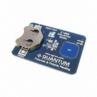
E100S
Manufacturer Part Number
E100S
Description
KIT EVAL FOR QT100
Manufacturer
Atmel
Series
Quantum, QTouch™r
Specifications of E100S
Sensor Type
Touch, Capacitive
Sensing Range
1 Button/Key
Interface
Logic Level
Voltage - Supply
3V
Embedded
No
Utilized Ic / Part
QT100
Lead Free Status / RoHS Status
Lead free / RoHS Compliant
Sensitivity
-
Lead Free Status / Rohs Status
Lead free / RoHS Compliant
For Use With/related Products
QT100-ISG
Other names
427-1128


2.9.2 HeartBeat™ Output
The QT100 output has a HeartBeat™ ‘health’ indicator
superimposed on it in both LP and SYNC modes. This
operates by taking the output pin into a three-state mode for
15µs once before every QT burst. This output state can be
used to determine that the sensor is operating properly, or it
can be ignored, using one of several simple methods.
The HeartBeat indicator can be sampled by using a pull-up
resistor on the OUT pin, and feeding the resulting
positive-going pulse into a counter, flip flop, one-shot, or other
circuit. The pulses will only be visible when the chip is not
detecting a touch.
If the sensor is wired to a microcontroller as shown in
Figure 2.7, the microcontroller can reconfigure the load
resistor to either V
the QT100, so that the pulses are evident in either state.
Electromechanical devices like relays will usually ignore the
short Heartbeat pulse. The pulse also has too low a duty cycle
to visibly affect LEDs. It can be filtered completely if desired,
by adding an RC filter to the output, or if interfacing directly
and only to a high-impedance CMOS input, by doing nothing
or at most adding a small noncritical capacitor from OUT to
V
2.9.3 Output Drive
The OUT pin is active high and can sink or source up to 2mA.
When a large value of Cs (>20nF) is used the OUT current
should be limited to <1mA to prevent gain-shifting side effects,
which happen when the load current creates voltage drops on
the die and bonding wires; these small shifts can materially
influence the signal level to cause detection instability.
3 Circuit Guidelines
3.1 Application Note
Refer to Application Note AN-KD02, downloadable from the
Quantum website for more information on construction and
design methods. Go to http://www.qprox.com, click the
Support tab and then Application Notes.
3.2 Sample Capacitor
Cs is the charge sensing sample capacitor. The required Cs
value depends on the thickness of the panel and its dielectric
constant. Thicker panels require larger values of Cs. Typical
values are 2nF to 50nF depending on the sensitivity required;
larger values of Cs demand higher stability and better
dielectric to ensure reliable sensing.
lQ
SS
.
SS
or V
DD
depending on the output state of
6
The Cs capacitor should be a stable type, such as X7R
ceramic or PPS film. For more consistent sensing from unit to
unit, 5 percent tolerance capacitors are recommended. X7R
ceramic types can be obtained in 5 percent tolerance at little
or no extra cost. In applications where high sensitivity (long
burst length) is required the use of PPS capacitors is
recommended.
3.3 Power Supply, PCB Layout
The power supply can range between 2.0V and 5.5V. At 3V
current drain averages less than 500µA in Fast mode.
If the power supply is shared with another electronic system,
care should be taken to ensure that the supply is free of digital
spikes, sags, and surges which can adversely affect the
QT100. The QT100 will track slow changes in V
be badly affected by rapid voltage fluctuations. It is highly
recommended that a separate voltage regulator be used just
for the QT100 to isolate it from power supply shifts caused by
other components.
If desired, the supply can be regulated using a Low Dropout
(LDO) regulator, although such regulators often have poor
transient line and load stability. See Application Note
AN-KD02 (see Section 3.1) for further information on power
supply considerations.
Parts placement: The chip should be placed to minimize the
SNSK trace length to reduce low frequency pickup, and to
reduce stray Cx which degrades gain. The Cs and Rs
resistors (see Figure 1.1) should be placed as close to the
body of the chip as possible so that the trace between Rs and
the SNSK pin is very short, thereby reducing the antenna-like
ability of this trace to pick up high frequency signals and feed
them directly into the chip. A ground plane can be used under
the chip and the associated discretes, but the trace from the
Rs resistor and the electrode should not run near ground to
reduce loading.
For best EMC performance the circuit should be made entirely
with SMT components.
Electrode trace routing: Keep the electrode trace (and the
electrode itself) away from other signal, power, and ground
traces including over or next to ground planes. Adjacent
switching signals can induce noise onto the sensing signal;
any adjacent trace or ground plane next to, or under, the
electrode trace will cause an increase in Cx load and
desensitize the device.
Important Note: for proper operation a 100nF (0.1µF)
ceramic bypass capacitor must be used directly between
V
V
bypass capacitor should be placed very close to the
device’s power pins.
DD
DD
and V
transients; for example, during an ESD event. The
SS
, to prevent latch-up if there are substantial
QT100_3R0.09_0707
DD
, but it can
Related parts for E100S
Image
Part Number
Description
Manufacturer
Datasheet
Request
R

Part Number:
Description:
DEV KIT FOR AVR/AVR32
Manufacturer:
Atmel
Datasheet:

Part Number:
Description:
INTERVAL AND WIPE/WASH WIPER CONTROL IC WITH DELAY
Manufacturer:
ATMEL Corporation
Datasheet:
Part Number:
Description:
Low-Voltage Voice-Switched IC for Hands-Free Operation
Manufacturer:
ATMEL Corporation
Datasheet:
Part Number:
Description:
MONOLITHIC INTEGRATED FEATUREPHONE CIRCUIT
Manufacturer:
ATMEL Corporation
Datasheet:
Part Number:
Description:
AM-FM Receiver IC U4255BM-M
Manufacturer:
ATMEL Corporation
Datasheet:
Part Number:
Description:
Monolithic Integrated Feature Phone Circuit
Manufacturer:
ATMEL Corporation
Datasheet:
Part Number:
Description:
Multistandard Video-IF and Quasi Parallel Sound Processing
Manufacturer:
ATMEL Corporation
Datasheet:
Part Number:
Description:
High-performance EE PLD
Manufacturer:
ATMEL Corporation
Datasheet:
Part Number:
Description:
8-bit Flash Microcontroller
Manufacturer:
ATMEL Corporation
Datasheet:
Part Number:
Description:
2-Wire Serial EEPROM
Manufacturer:
ATMEL Corporation
Datasheet: