LM3433SQ-36AEV/NOPB National Semiconductor, LM3433SQ-36AEV/NOPB Datasheet - Page 8
LM3433SQ-36AEV/NOPB
Manufacturer Part Number
LM3433SQ-36AEV/NOPB
Description
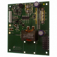
BOARD EVALUATION FOR LM3433SQ
Manufacturer
National Semiconductor
Series
PowerWise®r
Specifications of LM3433SQ-36AEV/NOPB
Current - Output / Channel
30A
Outputs And Type
1, Non-Isolated
Voltage - Output
6V
Features
Dimmable
Voltage - Input
-9 ~ -14V
Utilized Ic / Part
LM3433
Lead Free Status / RoHS Status
Lead free / RoHS Compliant
Other names
LM3433SQ-36AEV
Available stocks
Company
Part Number
Manufacturer
Quantity
Price
Company:

Part Number:
LM3433SQ-36AEV/NOPB
Manufacturer:
National Semiconductor
Quantity:
135


www.national.com
Operation
CURRENT REGULATOR OPERATION
The LM3433 is a controller for a Continuous Conduction Buck
Converter. Because of its buck topology and operation in the
continuous mode, the output current is very well controlled. It
only varies within a switching frequency cycle by the inductor
ripple current. This ripple current is normally set at 10% of the
DC current. Setting the ripple current lower than 10% is a
useful tradeoff of inductor size for less LED light output ripple.
Additional circuitry can be added to achieve any LED light
ripple desired.
The LED current is set by the voltage across a sense resistor.
This sense voltage is nominally 60mV but can be pro-
grammed higher or lower by an external control voltage.
The running frequency of the converter is programmed by an
external RC network in conjunction with the LED's forward
voltage. The frequency is nominally set around 200kHz to
500khz. Fast PWM control is available by shorting the output
of the current source by a MOSFET in parallel with the LED.
During the LED OFF time the running frequency is determined
by the RC network and the parasitic resistance of the output
circuit including the DIM FET R
The LM3433 system has been evaluated to be a very accu-
rate, high compliance current source. This is manifest in its
high output impedance and accurate current control. The cur-
rent is measured to vary less than 6mA out of 6A when
transitioning from LED OFF (output shorted) to LED ON (out-
put ~6V).
PROTECTION
The LM3433 has dedicated protection circuitry running during
normal operation. The thermal shutdown circuitry turns off all
power devices when the die temperature reaches excessive
levels. The V
protects the power devices during power supply startup and
shutdown to prevent operation at voltages less than the min-
imum operating input voltage. The V
protected to V
which decreases the supply current to approximately 35µA.
The ADJ, EN, and DIM pins are capable of sustaining up to
+/-2mA. If the voltages on these pins will exceed either V
CGND by necessity or by a potential fault, an external resistor
is recommended for protection. Size this resistor to limit pin
current to under 2mA. A 10k resistor should be sufficient. This
resistor may be used in any application for added protection
without any impact on function or performance.
DESIGN PROCEDURE
This section presents guidelines for selecting external com-
ponents.
SETTING LED CURRENT CONTROL
LM3433 uses average current mode control to regulate the
current delivered to the LED (I
resistor (R
I
and CSN pins. CSP and CSN are the inputs to an error am-
plifier with a programmed input offset voltage (V
V
tion:
LED
SENSE
into a voltage that is sensed by the LM3433 at the CSP
is used to regulate I
SENSE
EE
CC
. The LM3433 also features a shutdown mode
) in series with the LED is used to convert
undervoltage lockout (UVLO) comparator
LED
LED
DSON
based on the following equa-
). An external current sense
.
CC
pin is short circuit
SENSE
IN
or
).
8
FIXED LED CURRENT
The ADJ pin sets V
internal reference for V
current based on the following equation:
ADJUSTABLE LED CURRENT
When tied to an external voltage the ADJ pin sets V
based on the following equation:
When the reference on ADJ is adjustable, V
can be adjusted within the linear range of the ADJ pin. This
range has the following limitations:
When V
anteed by design to be less than or equal to 0.3V/16.667.
When V
V
equal to V
V
INPUT CAPACITOR SELECTION
A low ESR ceramic capacitor is needed to bypass the MOS-
FETs. This capacitor is connected between the drain of the
synchronous FET (CGND) and the source of the main switch
(V
appearing at the V
minimum with X5R or X7R dielectric. In addition to the FET
bypass capacitors, additional bypass capacitors should be
placed near the V
CGND.
The input capacitor must also be sized to handle the dimming
frequency input ripple when the DIM function is used. This
ripple may be as high as 85% of the nominal DC input current
(at 50% duty cycle). When dimming this input capacitor
should be selected to handle the input ripple current.
RECOMMENDED OPERATING FREQUENCY AND ON
TIME "TIME
Although the switching frequency can be set over a wide
range, the following equation describes the recommended
frequency selection given inexpensive magnetic materials
available today:
In the above equation A=1.2 for powdered iron core inductors
and A=0.9 or less for ferrite core inductors. This difference
takes into account the fact that ferrite cores generally become
more lossy at higher frequencies. Given the switching fre-
quency f calculated above, TIME
V
en, TIME
IN
SENSE
LED
EE
- 1V, V
). This capacitor prevents large voltage transients from
is the forward voltage drop of the LED that is being driv-
switches to 60mV.
ADJ
ADJ
ON
SENSE
ADJ
is less than this linear range the V
can be calculated with the following equation:
is greater than this linear range and less than
ON
/16.667. If V
" CALCULATION
is guaranteed by design to be less than or
EE
SENSE
EE
and V
pin of the LM3433. Use a 22µF value
SENSE
. Tie ADJ to V
IN
ADJ
. Select R
pins and should be returned to
is greater than V
ON
IN
can be calculated. If
SENSE
to use a fixed 60mV
SENSE
to fix the LED
SENSE
IN
and I
is guar-
SENSE
- 1V,
LED
Related parts for LM3433SQ-36AEV/NOPB
Image
Part Number
Description
Manufacturer
Datasheet
Request
R

Part Number:
Description:
IC LED DRIVER HIGH BRIGHT 24-LLP
Manufacturer:
National Semiconductor
Datasheet:

Part Number:
Description:
LM3433SQ-14A EVAL BOARD
Manufacturer:
National Semiconductor
Part Number:
Description:
BOARD, EVAL, 4A-20A, LED DVR, LM3433
Manufacturer:
National Semiconductor
Datasheet:
Part Number:
Description:
Common Anode Capable High Brightness LED Driver with High Frequency Dimming
Manufacturer:
National Semiconductor
Datasheet:
Part Number:
Description:
LM3433 Common Anode Capable High Brightness LED Driver with High Frequency Dimming; ; Qty per Container: 1
Manufacturer:
National Semiconductor
Datasheet:
Part Number:
Description:
National Semiconductor [8-Bit D/A Converter]
Manufacturer:
National Semiconductor
Datasheet:
Part Number:
Description:
National Semiconductor [Media Coprocessor]
Manufacturer:
National Semiconductor
Datasheet:
Part Number:
Description:
Digitally Controlled Tone and Volume Circuit with Stereo Audio Power Amplifier, Microphone Preamp Stage and National 3D Sound
Manufacturer:
National Semiconductor
Datasheet:
Part Number:
Description:
Digitally Controlled Tone and Volume Circuit with Stereo Audio Power Amplifier, Microphone Preamp Stage and National 3D Sound
Manufacturer:
National Semiconductor
Datasheet:
Part Number:
Description:
AC97 Rev 2 Codec with Sample Rate Conversion and National 3D Sound
Manufacturer:
National Semiconductor
Part Number:
Description:
Manufacturer:
National Semiconductor
Datasheet:
Part Number:
Description:
Manufacturer:
National Semiconductor
Datasheet:
Part Number:
Description:
General Purpose, Low Voltage, Low Power, Rail-to-Rail Output Operational Amplifiers
Manufacturer:
National Semiconductor
Datasheet:
Part Number:
Description:
8-bit 20 MSPS flash A/D converter.
Manufacturer:
National Semiconductor
Datasheet: