LM3407EVAL National Semiconductor, LM3407EVAL Datasheet - Page 3
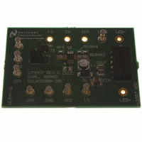
LM3407EVAL
Manufacturer Part Number
LM3407EVAL
Description
BOARD EVALUATION FOR LM3407
Manufacturer
National Semiconductor
Series
PowerWise®r
Specifications of LM3407EVAL
Current - Output / Channel
350mA
Outputs And Type
1, Non-Isolated
Voltage - Output
4.5V
Features
Dimmable
Voltage - Input
4.5 ~ 30V
Utilized Ic / Part
LM3407
Lead Free Status / RoHS Status
Contains lead / RoHS non-compliant


SYSTEM PARAMETERS
INTERNAL VOLTAGE REGULATOR
N-MOSFET DRIVER
CONTROL LOOP
VIN to GND
VIN to GND (Transient)
LX to GND
LX to GND (Transient)
ISNS, FS, DIM, EN to GND
ESD Rating
Human Body Model (Note 2)
Absolute Maximum Ratings
If Military/Aerospace specified devices are required,
please contact the National Semiconductor Sales Office/
Distributors for availability and specifications.
Electrical Characteristics
for T
specification limits are guaranteed by design, test, or statistical analysis.
Note 1: Absolute Maximum Ratings are limits beyond which damage to the device may occur. Operating Ratings are conditions under which operation of the
device is intended to be functional. For guaranteed specifications and test conditions, see the Electrical Characteristics.
Note 2: The human body model is a 100pF capacitor discharged through a 1.5kΩ resistor into each pin.
Note 3: θ
Note 4: Typical specification represent the most likely parametric norm at 25°C operation.
Note 5: V
V
Symbol
T
R
UVLO-HYS
V
t
V
A
V
V
V
ON-MIN
I
SD-HYS
DS(ON)
SHUT
T
V
A
DIM_H
DIM_L
f
UVLO
EN_H
= T
EN_L
I
I
SW
IN
SD
CC
Q
EA
JA
CC
J
of 50°C/W with thermal pad, EP soldered to a minimum of 2 square inches of 1 oz. Copper on the top or bottom PCB layer.
provides self bias for the internal gate drive and control circuits. Device thermal limitations limit external loading to the pin.
= 25°C (Note 4). Limits appearing in boldface type apply over full Operating Temperature Range. Datasheet min/max
Parameter
Operating Input Current
Quiescent Input current
Shutdown Input Current
Input Under Voltage Lock-out Threshold V
UVLO Hysteresis
EN pin HIGH Threshold
EN pin LOW Threshold
DIM pin HIGH Threshold
DIM pin LOW Threshold
Switching Frequency
Minimum On-time
Thermal Shutdown Threshold
Thermal Shutdown Hysteresis
VCC Regulator Output Voltage (Note 5) V
Main Switch ON Resistance
Error Amp Open Loop Gain
-3V (2 ns), 42V (500 ms)
V
IN
42V (500 ms)
(Note 1)
-0.3V to 36V
-0.3V to 36V
= 12V unless otherwise indicated. Typical and limits appearing in plain type apply
-0.3V to 7V
2kV
Conditions
4.5V
V
4.5V
V
V
V
V
V
V
V
R
R
I
sink
EN
EN
EN
IN
IN
EN
EN
DIM
DIM
IN
T
T
= 80 kΩ
= 40 kΩ
3
Rising
Falling
= 12V
= 80mA
= 5V, V
= 5V, V
= 0V
Rising
Falling
Rising
Falling
≤
≤
Junction Temperature
Storage Temperature
Soldering Information
Lead Temperature (Soldering,
10sec)
Infrared or Convection (20sec)
V
V
V
Junction Temperature Range
Thermal Resistance (θ
Operating Ratings
IN
IN
IN
≤
≤
PWM
PWM
30V
30V
= 5V, LX = open
= 0V
JA
) (Note 3)
0.58
0.20
Min
1.3
1.3
36
1000
0.78
0.27
1.75
1.75
0.77
Typ
200
500
200
165
3.6
1.9
1.9
4.5
48
25
60
−40°C to + 125°C
−65°C to + 125°C
Max
0.98
0.39
1.45
www.national.com
4.5V to 30V
4.5
2.4
2.4
60
50°C/W
150°C
260°C
235°C
Units
kHz
mA
mA
mV
µA
dB
ns
°C
°C
Ω
V
V
V
V
V
V
Related parts for LM3407EVAL
Image
Part Number
Description
Manufacturer
Datasheet
Request
R

Part Number:
Description:
Precision Fahrenheit Temperature Sensors
Manufacturer:
National Semiconductor
Part Number:
Description:
National Semiconductor [8-Bit D/A Converter]
Manufacturer:
National Semiconductor
Datasheet:
Part Number:
Description:
National Semiconductor [Media Coprocessor]
Manufacturer:
National Semiconductor
Datasheet:
Part Number:
Description:
Digitally Controlled Tone and Volume Circuit with Stereo Audio Power Amplifier, Microphone Preamp Stage and National 3D Sound
Manufacturer:
National Semiconductor
Datasheet:
Part Number:
Description:
Digitally Controlled Tone and Volume Circuit with Stereo Audio Power Amplifier, Microphone Preamp Stage and National 3D Sound
Manufacturer:
National Semiconductor
Datasheet:
Part Number:
Description:
AC97 Rev 2 Codec with Sample Rate Conversion and National 3D Sound
Manufacturer:
National Semiconductor
Part Number:
Description:
Manufacturer:
National Semiconductor
Datasheet:
Part Number:
Description:
Manufacturer:
National Semiconductor
Datasheet:
Part Number:
Description:
General Purpose, Low Voltage, Low Power, Rail-to-Rail Output Operational Amplifiers
Manufacturer:
National Semiconductor
Datasheet:
Part Number:
Description:
8-bit 20 MSPS flash A/D converter.
Manufacturer:
National Semiconductor
Datasheet:
Part Number:
Description:
Low Noise Quad Operational Amplifier
Manufacturer:
National Semiconductor
Datasheet:
Part Number:
Description:
Quad Differential Line Receivers
Manufacturer:
National Semiconductor
Datasheet:
Part Number:
Description:
Quad High Speed Trapezoidal? Bus Transceiver
Manufacturer:
National Semiconductor
Datasheet:
Part Number:
Description:
Dual Line Receiver
Manufacturer:
National Semiconductor
Datasheet: