LM20134EVAL National Semiconductor, LM20134EVAL Datasheet - Page 15
LM20134EVAL
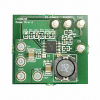
Manufacturer Part Number
LM20134EVAL
Description
BOARD EVAL 4A POWERWISE LM20134
Manufacturer
National Semiconductor
Series
PowerWise®r
Specifications of LM20134EVAL
Main Purpose
DC/DC, Step Down
Outputs And Type
1, Non-Isolated
Voltage - Output
1.2V
Current - Output
4A
Voltage - Input
2.95 ~ 5.5V
Regulator Topology
Buck
Board Type
Fully Populated
Utilized Ic / Part
LM20134
Lead Free Status / RoHS Status
Not applicable / Not applicable
Power - Output
-
Frequency - Switching
-


To achieve a -20dB/decade slope, the error amplifier zero,
located at f
pole (f
can be added to cancel the output filter zero at (f
cellation of the output filter zero is recommended if larger
value, non-ceramic output capacitors are used.
Compensation of the LM20134 is achieved by adding an RC
network as shown in Figure 5 below.
A good starting value for C
Once the value of C
calculated using the equation below to cancel the output filter
pole (f
A higher crossover frequency can be obtained, usually at the
expense of phase margin, by lowering the value of C
recalculating the value of R
recalculating R
lower crossover frequency. As with any attempt to compen-
sate the LM20134 the stability of the system should be verified
for desired transient droop and settling time.
If the output filter zero, (f
quency (F
at the COMP pin to ground. This capacitor adds a pole to
cancel the output filter zero assuring the crossover frequency
will occur before the double pole at f
margin. The output filter zero is set by the output capacitor
value and ESR as shown in the equation below.
If needed, the value for C
equation shown below.
Where R
R
AVIN FILTERING COMPONENTS (C
To prevent high frequency noise spikes from disturbing the
sensitive analog circuitry connected to the AVIN and AGND
pins, a high frequency RC filter is required between PVIN and
AVIN. These components are shown in Figure 2 as C
C1
is the calculated compensation resistance.
FIGURE 5. Compensation Network for LM20134
P(FIL)
P(FIL)
ESR
C
). An additional error amp pole, located at f
) as shown in Figure 4.
Z(EA)
), an additional capacitor (C
is the output capacitor series resistance and
C1
, should positioned to cancel the output filter
will provide additional phase margin at a
C1
is chosen the value of RC should be
Z(FIL)
C2
C1
C1
) approaches the crossover fre-
. Likewise, increaseing C
should be calculated using the
for most applications is 4.7 nF.
SW
30030414
F
/2 degrades the phase
C2
and R
) should be placed
F
)
Z(FIL)
). Can-
C1
C1
P2(EA)
F
and
and
and
,
15
R
ommended value of C
should be placed as close to the IC as possible with a direct
connection from AVIN to AGND. A good quality X5R or X7R
ceramic capacitor should be used for C
SUB-REGULATOR BYPASS CAPACITOR (C
The capacitor at the VCC pin provides noise filtering and sta-
bility for the internal sub-regulator. The recommended value
of C
10 µF. The capacitor should be a good quality ceramic X5R
or X7R capacitor. In general, a 1 µF ceramic capacitor is rec-
ommended for most applications.
SETTING THE START UP TIME (C
The addition of a capacitor connected from the SS pin to
ground sets the time at which the output voltage will reach the
final regulated value. Larger values for C
start up times. Table 3, shown below provides a list of soft
start capacitors and the corresponding typical start up times.
If different start up times are needed the equation shown be-
low can be used to calculate the start up time.
As shown above, the start up time is influenced by the value
of the Soft-Start capacitor C
current I
istics table.
While the Soft-Start capacitor can be sized to meet many start
up requirements, there are limitations to its size. The Soft-
Start time can never be faster than 1ms due to the internal
default 1ms start up time. When the device is enabled there
is an approximate time interval of 50 µs when the Soft-Start
capacitor will be discharged just prior to the Soft-Start ramp.
If the enable pin is rapidly pulsed or the Soft-Start capacitor
is large there may not be enough time for C
discharge resulting in start up times less than predicted. To
aid in discharging the Soft-Start capacitor during long disable
periods an external 1 MΩ resistor from SS/TRK to ground can
be used without greatly affecting the start-up time.
USING PRECISION ENABLE AND POWER GOOD
The precision enable(EN) and power good(PGOOD) pins of
the LM20134 can be used to address many sequencing re-
quirements. The turn-on of the LM20134 can be controlled
with the precision enable pin by using two external resistors
as shown in Figure 6
F
. The required value for R
VCC
TABLE 3. Start Up Times for Different Soft-Start
Start Up Time (ms)
should be no smaller than 1 µF and no greater than
SS
(A). that may be found in the electrical character-
10
15
20
1
5
F
Capacitors
is 1.0 µF. The filter capacitor, C
SS
F
(F) and the 5 µA Soft-Start pin
is 1Ω. C
SS
)
F
F
SS
.
must be used. Rec-
C
will result in longer
SS
none
100
120
33
68
SS
(nF)
VCC
to completely
www.national.com
)
F
Related parts for LM20134EVAL
Image
Part Number
Description
Manufacturer
Datasheet
Request
R

Part Number:
Description:
MODULE TXRX BLUETOOTH 2 18SMD
Manufacturer:
Flexipanel
Datasheet:

Part Number:
Description:
MODULE TXRX BLUETOOTH 2 18DIP
Manufacturer:
Flexipanel
Datasheet:

Part Number:
Description:
LM20 2.4V, 10?A, SC70, micro SMD Temperature Sensor
Manufacturer:
National Semiconductor
Datasheet:
Part Number:
Description:
National Semiconductor [8-Bit D/A Converter]
Manufacturer:
National Semiconductor
Datasheet:
Part Number:
Description:
National Semiconductor [Media Coprocessor]
Manufacturer:
National Semiconductor
Datasheet:
Part Number:
Description:
Digitally Controlled Tone and Volume Circuit with Stereo Audio Power Amplifier, Microphone Preamp Stage and National 3D Sound
Manufacturer:
National Semiconductor
Datasheet:
Part Number:
Description:
Digitally Controlled Tone and Volume Circuit with Stereo Audio Power Amplifier, Microphone Preamp Stage and National 3D Sound
Manufacturer:
National Semiconductor
Datasheet:
Part Number:
Description:
AC97 Rev 2 Codec with Sample Rate Conversion and National 3D Sound
Manufacturer:
National Semiconductor
Part Number:
Description:
Manufacturer:
National Semiconductor
Datasheet:
Part Number:
Description:
Manufacturer:
National Semiconductor
Datasheet:
Part Number:
Description:
General Purpose, Low Voltage, Low Power, Rail-to-Rail Output Operational Amplifiers
Manufacturer:
National Semiconductor
Datasheet:
Part Number:
Description:
8-bit 20 MSPS flash A/D converter.
Manufacturer:
National Semiconductor
Datasheet:
Part Number:
Description:
Low Noise Quad Operational Amplifier
Manufacturer:
National Semiconductor
Datasheet:
Part Number:
Description:
Quad Differential Line Receivers
Manufacturer:
National Semiconductor
Datasheet: