STEVAL-ISA053V2 STMicroelectronics, STEVAL-ISA053V2 Datasheet - Page 42
STEVAL-ISA053V2
Manufacturer Part Number
STEVAL-ISA053V2
Description
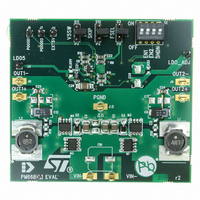
BOARD EVALUATION FOR PM6680A
Manufacturer
STMicroelectronics
Type
DC/DC Switching Converters, Regulators & Controllersr
Specifications of STEVAL-ISA053V2
Design Resources
STEVAL-ISA053V2 Gerber Files PM6680A Eval Kit Schematic STEVAL-ISA053V2 Bill of Material
Main Purpose
DC/DC, Step Down with LDO
Outputs And Type
3, Non-Isolated
Voltage - Output
1.8V, 3.3V, 5V
Current - Output
2.5A, 2.5A, 100mA
Voltage - Input
6 ~ 28V
Regulator Topology
Buck
Frequency - Switching
200kHz, 300kHz
Board Type
Fully Populated
Utilized Ic / Part
PM6680A
Input Voltage
6 V to 36 V
Output Voltage
5 V
Product
Power Management Modules
Lead Free Status / RoHS Status
Lead free / RoHS Compliant
Power - Output
-
Lead Free Status / Rohs Status
Lead free / RoHS Compliant
For Use With/related Products
PM6680A
Other names
497-6379
Available stocks
Company
Part Number
Manufacturer
Quantity
Price
Company:

Part Number:
STEVAL-ISA053V2
Manufacturer:
STMicroelectronics
Quantity:
1


Design guidelines
42/48
Equation 41
5.
6.
7.
8.
9.
●
●
●
●
(Let's assume Tmax=75 °C in R
R
Input capacitor
Maximum input capacitor RMS current is about 1.084 A. Then I
We put two 10 µF ceramic capacitors with Irms = 1.5 A.
Synchronous rectifier
OUT1: Shottky diode STPS1L40M
OUT2: Shottky diode STPS1L40M
Integrator loop
(Refer to figure 14)
OUT1: The ripple is smaller than 40 mV, then the virtual ESR network is required.
C
OUT2: The ripple is smaller than 40 mV, then the virtual ESR network is required.
C
Output feedback divider
(Refer to figure 6)
OUT1: R1 = 10 kΩ; R2 = 27 kΩ
OUT2: R1 = 10 kΩ; R2 = 10 kΩ
Layout guidelines
The layout is very important in terms of efficiency, stability and noise of the system. It is
possible to refer to the PM6680A demoboard for a complete layout example.
For good PC board layout follows these guidelines:
Place on the top side all the power components (inductors, input and output capacitors,
MOSFETs and diodes). Refer them to a power ground plan, PGND. If possible, reserve
a layer to PGND plan. The PGND plan is the same for both the switching sections.
AC current paths layout is very critical (see
their length. Trace the LS MOSFET connection to PGND plan as short as possible.
Place the synchronous diode D near the LS MOSFET. Connect the LS MOSFET drain
to the switching node with a short trace.
Place input capacitors near HS MOSFET drain. It is recommended to use the same
input voltage plan for both the switching sections, in order to put together all input
capacitors.
Place all the sensitive analog signals (feedbacks, voltage reference, current sense
paths) on the bottom side of the board or in an inner layer. Isolate them from the power
top side with a signal ground layer, SGND. Connect the SGND and PGND plans only in
one point (a multiple vias connection is preferable to a 0 ohm resistor connection) near
the PGND device pin. Place the device on the top or on the bottom size and connect
the exposed pad and the SGND pins to the SGND plan (see
CSENSE
INT
INT
= 1.5 nF; C
=1.5 nF; C
= 560 Ω.
filt
filt
=47 pF; R
= 47 pF; R
INT
INT
= 820 Ω
DSon
= 1.1 kΩ
calculation). We choose standard value
Figure 41
). The first priority is to minimize
Figure 41
CINRMS
).
> 1.084 A
PM6680A
Related parts for STEVAL-ISA053V2
Image
Part Number
Description
Manufacturer
Datasheet
Request
R

Part Number:
Description:
BOARD RGB CTR ST7,STP08C596MTR
Manufacturer:
STMicroelectronics
Datasheet:

Part Number:
Description:
Power Management IC Development Tools Full Speed USB to RS232 Bridge Demo
Manufacturer:
STMicroelectronics
Datasheet:
Part Number:
Description:
Power Management IC Development Tools 2.5W solar eval BRD USB SPV1040 LD39050
Manufacturer:
STMicroelectronics
Datasheet:

Part Number:
Description:
BOARD EVAL FOR MEMS SENSORS
Manufacturer:
STMicroelectronics
Datasheet:

Part Number:
Description:
KIT DEV STARTER ST10F276Z5
Manufacturer:
STMicroelectronics
Datasheet:

Part Number:
Description:
BOARD EVAL HDMI $ VIDEO SWITCH
Manufacturer:
STMicroelectronics
Datasheet:

Part Number:
Description:
BOARD DEMO ACCELEROMETER DIL24
Manufacturer:
STMicroelectronics
Datasheet:

Part Number:
Description:
BOARD STLM75/STDS75/ST72F651
Manufacturer:
STMicroelectronics
Datasheet:

Part Number:
Description:
EVAL BOARD 3AXIS MEMS ACCELLRMTR
Manufacturer:
STMicroelectronics
Datasheet:

Part Number:
Description:
BOARD EVAL 8BIT MICRO + TDE1708
Manufacturer:
STMicroelectronics
Datasheet:
Part Number:
Description:
STMicroelectronics [RIPPLE-CARRY BINARY COUNTER/DIVIDERS]
Manufacturer:
STMicroelectronics
Datasheet:
Part Number:
Description:
STMicroelectronics [LIQUID-CRYSTAL DISPLAY DRIVERS]
Manufacturer:
STMicroelectronics
Datasheet:
Part Number:
Description:
BOARD EVAL FOR MEMS SENSORS
Manufacturer:
STMicroelectronics
Datasheet: