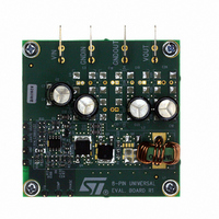
STEVAL-ISA027V1 STMicroelectronics, STEVAL-ISA027V1 Datasheet - Page 15

STEVAL-ISA027V1
Manufacturer Part Number
STEVAL-ISA027V1
Description
BOARD EVAL 1PH STPDN CONV L6726A
Manufacturer
STMicroelectronics
Type
DC/DC Switching Converters, Regulators & Controllersr
Specifications of STEVAL-ISA027V1
Design Resources
STEVAL-ISA027V1 Gerber Files STEVAL-ISA027V1 Schematic STEVAL-ISA027V1 Bill of Material
Main Purpose
DC/DC, Step Down
Outputs And Type
1, Non-Isolated
Voltage - Output
1.25V
Current - Output
20A
Voltage - Input
5 ~ 12V
Regulator Topology
Buck
Frequency - Switching
270kHz
Board Type
Fully Populated
Utilized Ic / Part
L6726A
Input Voltage
5 V to 12 V
Output Voltage
1.25 V
Product
Power Management Modules
Lead Free Status / RoHS Status
Lead free / RoHS Compliant
Power - Output
-
Lead Free Status / Rohs Status
Lead free / RoHS Compliant
For Use With/related Products
L6726A
Other names
497-6259
L6726A
8
8.1
8.2
Application details
Output voltage selection
L6726A is capable to precisely regulate an output voltage as low as 0.8 V. In fact, the device
comes with a fixed 0.8 V internal reference that guarantees the output regulated voltage to
be within ±1% tolerance over line and temperature variations between 0 °C and 70 °C
(excluding output resistor divider tolerance, when present).
Output voltage higher than 0.8 V can be achieved by adding a resistor R
and ground. Referring to
where V
Compensation network
The control loop shown in
transconductance type with fixed gain (3.3 ms typ.). The FB voltage is regulated to the
internal reference, thus the output voltage is fixed accordingly to the output resistor divider
(when present).
Transconductance error amplifier output current generates a voltage across Z
compared to oscillator saw-tooth waveform to provide PWM signal to the driver section.
PWM signal is then transferred to the switching node with V
filtered by the output filter.
Figure 8.
The converter transfer function is the small signal transfer function between the voltage at
the output node of the EA (COMP) and V
conjugate) at frequency F
REF
is 0.8 V.
PWM control loop
ΔV
OSC
OSC
Figure
LC
Figure 8
C
R
depending on the L-C
F
COMPARATOR
F
V
Doc ID 12754 Rev 4
COMP
1, the steady state DC output voltage will be:
OUT
_
+
PWM
is a voltage mode control loop. The error amplifier is a
Z
C
F
=
P
OTA
V
OUT
REF
. This function has a double pole (complex
+
_
⋅
⎛
⎝
V
OUT
1
V
IN
R
REF
FB
+
OS
resonance and a zero at F
---------- -
R
R
L
OS
FB
R
FB
IN
⎞
⎠
amplitude. This waveform is
OUTPUT
DIVIDER
R
C
ESR
OUT
Application details
OS
V
OUT
between FB pin
F
, which is
ESR
15/35


