CDB35L00 Cirrus Logic Inc, CDB35L00 Datasheet - Page 2
CDB35L00
Manufacturer Part Number
CDB35L00
Description
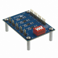
DEVELOPMENT BOARD FOR CS35L0X
Manufacturer
Cirrus Logic Inc
Datasheet
1.CDB35L00.pdf
(12 pages)
Specifications of CDB35L00
Amplifier Type
Class D
Output Type
4-Channel (Quad)
Max Output Power X Channels @ Load
2.7W x 4 @ 4 Ohm
Voltage - Supply
2.5 V ~ 5.5 V
Board Type
Fully Populated
Utilized Ic / Part
CS35L0X
Description/function
Audio Amplifiers
Operating Supply Voltage
2.5 V to 5.5 V
Output Power
1.6 W, 2.7 W
Product
Audio Modules
For Use With/related Products
CS35L00
Lead Free Status / RoHS Status
Contains lead / RoHS non-compliant
Operating Temperature
-
Lead Free Status / Rohs Status
Lead free / RoHS Compliant
Other names
598-1803


2
TABLE OF CONTENTS
LIST OF FIGURES
LIST OF TABLES
1. SYSTEM OVERVIEW ............................................................................................................................. 3
2. GROUNDING AND POWER SUPPLY DECOUPLING .......................................................................... 7
3. SYSTEM CONNECTORS AND JUMPERS ............................................................................................ 8
4. CDB SCHEMATIC .................................................................................................................................. 9
5. CDB LAYOUT ....................................................................................................................................... 11
6. REVISION HISTORY ............................................................................................................................ 12
Figure 1.Hybrid Control Resistors ............................................................................................................... 4
Figure 2.Shutdown Control Resistors ......................................................................................................... 5
Figure 3.Optional Bypass Trace Cut Locations for U1 ................................................................................ 6
Figure 4.CDB35L00-X4 Schematic ............................................................................................................. 9
Figure 5.CDB35L00-X4 Top Side Component Placement ........................................................................ 11
Figure 6.CDB35L00-X4 Bottom Side Component Placement ................................................................... 11
Figure 7.CDB35L00-X4 Layer 1 Copper ................................................................................................... 11
Figure 8.CDB35L00-X4 Layer 2 Copper ................................................................................................... 11
Figure 9.CDB35L00-X4 Layer 3 Copper ................................................................................................... 11
Figure 10.CDB35L00-X4 Layer 4 Copper ................................................................................................. 11
Table 1. S1 Switch GAIN & MODE Configurations ..................................................................................... 3
Table 2. Hybrid Control Resistor & S1 Switch MODE Configurations ......................................................... 4
Table 3. S1 Switch Default Shutdown Configurations ................................................................................. 5
Table 4. System Input and Output Connections ......................................................................................... 8
Table 5. S1 Switch Settings ........................................................................................................................ 8
Table 6. Bill of Materials Listing ................................................................................................................ 10
1.1 CS35L00 Hybrid Class-D Amplifier .................................................................................................. 3
1.2 Power Supply ................................................................................................................................... 3
1.3 Operational Modes ........................................................................................................................... 3
1.4 Shutdown Control ............................................................................................................................ 4
1.5 Gain Control ..................................................................................................................................... 5
1.6 Differential Analog Inputs ................................................................................................................. 6
1.7 Speaker Outputs .............................................................................................................................. 6
2.1 Power Supply Decoupling ................................................................................................................ 7
2.2 Electromagnetic Interference (EMI) ................................................................................................. 7
4.1 Bill of Materials ............................................................................................................................... 10
1.3.1 Operational Mode Control ....................................................................................................... 3
1.4.1 Shutdown Control Resistors .................................................................................................... 5
1.5.1 Optional Gain Adjustment Resistors ....................................................................................... 5
1.7.1 Optional Speaker Output EMI Filter Components ................................................................... 6
2.2.1 Suppression of EMI at the Source ........................................................................................... 7
CDB35L00-X4
DS913DB2
Related parts for CDB35L00
Image
Part Number
Description
Manufacturer
Datasheet
Request
R

Part Number:
Description:
Audio Modules & Development Tools Eval Bd - DF 4ch ADC 8ch DAC & 32bit DSP
Manufacturer:
Cirrus Logic Inc
Part Number:
Description:
Development Kit
Manufacturer:
Cirrus Logic Inc
Datasheet:
Part Number:
Description:
Development Kit
Manufacturer:
Cirrus Logic Inc
Datasheet:


Part Number:
Description:
High-efficiency PFC + Fluorescent Lamp Driver Reference Design
Manufacturer:
Cirrus Logic Inc
Datasheet:
Part Number:
Description:
Development Kit
Manufacturer:
Cirrus Logic Inc
Datasheet:
Part Number:
Description:
Development Kit
Manufacturer:
Cirrus Logic Inc
Datasheet:

Part Number:
Description:
Development Kit
Manufacturer:
Cirrus Logic Inc
Datasheet:
Part Number:
Description:
Development Kit
Manufacturer:
Cirrus Logic Inc
Datasheet:
Part Number:
Description:
Development Kit
Manufacturer:
Cirrus Logic Inc
Datasheet:

Part Number:
Description:
EVALUATION BOARD FOR CS8427
Manufacturer:
Cirrus Logic Inc
Datasheet:

Part Number:
Description:
BOARD EVAL FOR CS8416 RCVR
Manufacturer:
Cirrus Logic Inc
Datasheet:

Part Number:
Description:
EVALUATION BOARD FOR CS8420
Manufacturer:
Cirrus Logic Inc
Datasheet:

Part Number:
Description:
KIT DEVELOPMENT EP9315 ARM9
Manufacturer:
Cirrus Logic Inc
Datasheet:

Part Number:
Description:
KIT DEVELOPMENT EP9302 ARM9
Manufacturer:
Cirrus Logic Inc
Datasheet: