AD9516-3/PCBZ Analog Devices Inc, AD9516-3/PCBZ Datasheet - Page 9
AD9516-3/PCBZ
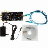
Manufacturer Part Number
AD9516-3/PCBZ
Description
BOARD EVAL FOR AD9516-3 2.0GHZ
Manufacturer
Analog Devices Inc
Specifications of AD9516-3/PCBZ
Main Purpose
Timing, Clock Generator
Embedded
No
Utilized Ic / Part
AD9516-3
Primary Attributes
2 Inputs, 14 Outputs, 2GHz VCO
Secondary Attributes
CMOS, LVDS, LVPECL Output Logic, ADIsimCLK™ Graphical User Interface
Silicon Manufacturer
Analog Devices
Application Sub Type
PLL Clock Synthesizer
Kit Application Type
Clock & Timing
Silicon Core Number
AD9516-0, AD9516-1, AD9516-2
Silicon Family Name
AD9516-X
Rohs Compliant
Yes
Lead Free Status / RoHS Status
Lead free / RoHS Compliant


Evaluation Board User Guide
REGISTER W/R BOX
The REGISTER W/R (write/read) box has four buttons and
three check boxes.
The WRITE button transfers the values stored in the evaluation
software to the evaluation board. It blinks red when register
values have changed.
The READ button transfers the values stored in the evaluation
board to the evaluation software.
The UPDATE button issues an I/O update command by writing
0x01 to Register 0x232.
Selecting the All check box transfers all of the registers when
the WRITE button is clicked. When this check box is cleared,
only the registers whose value has changed are written.
Selecting the Auto check box adjacent to the WRITE box
forces the evaluation software to write the register changes
to the evaluation board automatically when they occur.
Selecting the Auto check box adjacent to the UPDATE box
forces the evaluation software to issue an I/O update command
whenever registers are written to the AD951x. It is checked by
default.
SYNC, PD (POWER DOWN), AND RESET BUTTONS
The SYNC, PD, and RESET buttons allow you to control the
SYNC , PD, and RESET pins on the AD951x.
Each button has three options: Strobe, Latch, and Release.
Strobe activates the pin, and then releases it. Latch holds
the pin active until the Release command is issued.
REFERENCE (R) DIVIDER WINDOW
The R Divider window shown in Figure 12 is accessed by
clicking the R DIVIDER box on the main window. It allows
you to set the reference divider. If this box is colored gray, the
PLL is off. To turn the PLL on, click the PLL MODE box at
the top of the main window, and select Norm Op.
The R Divider window has a check box for holding the
R divider in reset. When the R divider is held in reset, the
PLL loop is opened. Therefore, this feature is seldom used.
Figure 12. R Divider Window
Rev. 0 | Page 9 of 16
R AND N DELAY WINDOW
The AD951x features two delay circuits (one on the reference
divider path, and one on the feedback divider path) that allow
the user to control the static phase offset between the reference
input and the PLL output. The R Path Delay window shown in
Figure 13 is accessed by clicking the R DELAY button on the
main screen. The R DELAY box is identical to the N DELAY
box. These delay settings allow you to vary the static phase
offset of the PLL.
FEEDBACK (N) DIVIDER WINDOW
The reference divider window shown in Figure 14 is accessed by
clicking the N DIVIDER box on the main screen. If this box is
colored gray, the PLL is off. To turn the PLL on, click the PLL
MODE box at the top of the main screen, and select Norm Op.
The various modes of the N divider are described in detail in
the AD951x data sheet. For most applications, the 8/9 or 16/17
dual modulus modes are used. For applications requiring a
divider value larger than 131,119, the 32/33 mode is provided.
Different applications require different settings, and you can
experiment with the different settings.
Figure 13. R Path Delay Window
Figure 14. N Divider Window
UG-075
Related parts for AD9516-3/PCBZ
Image
Part Number
Description
Manufacturer
Datasheet
Request
R

Part Number:
Description:
IC CLOCK PLL/VCO 2GHZ 64LFCSP
Manufacturer:
Analog Devices Inc
Datasheet:
Part Number:
Description:
IC CLOCK GEN 2.8GHZ VCO 64-LFCSP
Manufacturer:
Analog Devices Inc
Datasheet:
Part Number:
Description:
IC,Fourteen Distributed-Output Clock Driver,LLCC,64PIN,PLASTIC
Manufacturer:
Analog Devices Inc
Datasheet:
Part Number:
Description:
IC,Ten Distributed-Output Clock Driver,LLCC,64PIN,PLASTIC
Manufacturer:
Analog Devices Inc
Datasheet:
Part Number:
Description:
IC,Ten Distributed-Output Clock Driver,LLCC,64PIN,PLASTIC
Manufacturer:
Analog Devices Inc
Datasheet:
Part Number:
Description:
Clock IC With 1.8GHz On-chip VCO
Manufacturer:
Analog Devices Inc
Datasheet:

Part Number:
Description:
BOARD EVAL FOR AD9516-2 2.2GHZ
Manufacturer:
Analog Devices Inc
Datasheet:

Part Number:
Description:
Clock IC With 2.5GHz On-chip VCO EB
Manufacturer:
Analog Devices Inc
Datasheet:
Part Number:
Description:
IC CLOCK GEN 2.8GHZ VCO 64-LFCSP
Manufacturer:
Analog Devices Inc
Datasheet:
Part Number:
Description:
IC,Ten Distributed-Output Clock Driver,LLCC,64PIN,PLASTIC
Manufacturer:
Analog Devices Inc
Datasheet:
Part Number:
Description:
IC,Fourteen Distributed-Output Clock Driver,LLCC,64PIN,PLASTIC
Manufacturer:
Analog Devices Inc
Datasheet:
Part Number:
Description:
IC,Ten Distributed-Output Clock Driver,LLCC,64PIN,PLASTIC
Manufacturer:
Analog Devices Inc
Datasheet:
Part Number:
Description:
Clock IC With 1.8GHz On-chip VCO
Manufacturer:
Analog Devices Inc
Datasheet:
Part Number:
Description:
10/14 Chan Clock IC W/PLL-no VCO
Manufacturer:
Analog Devices Inc
Datasheet:
Part Number:
Description:
10/14 Chan Clock IC W/PLL-no VCO
Manufacturer:
Analog Devices Inc
Datasheet: