GS-R405S STMicroelectronics, GS-R405S Datasheet - Page 3
GS-R405S
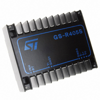
Manufacturer Part Number
GS-R405S
Description
IC REG SW STEP DOWN 4A 5.1V
Manufacturer
STMicroelectronics
Series
GS-R400r
Type
Point of Load (POL) Non-Isolatedr
Datasheet
1.GS-R400V.pdf
(5 pages)
Specifications of GS-R405S
Output
5.1V
Number Of Outputs
1
Power (watts)
20W
Mounting Type
Through Hole
Voltage - Input
9 ~ 46V
Package / Case
Module
1st Output
5.1 VDC @ 4A
Size / Dimension
3.37" L x 2.64" W x 0.84" H (85.5mm x 67mm x 21.3mm)
Power (watts) - Rated
20W
Operating Temperature
-20°C ~ 85°C
Efficiency
70%
Output Voltage
5.1 V
Output Current
4 A
Input Voltage
9 V to 46 V
Switching Frequency
100 KHz
Operating Temperature Range
- 20 C to + 85 C
Mounting Style
SMD/SMT
Lead Free Status / RoHS Status
Lead free / RoHS Compliant
3rd Output
-
2nd Output
-
Lead Free Status / Rohs Status
Lead free / RoHS Compliant
Other names
497-8273
GS-R405S
GS-R405S
Available stocks
Company
Part Number
Manufacturer
Quantity
Price
Company:

Part Number:
GS-R405S
Manufacturer:
STMicroelectronics
Quantity:
33
Company:
Part Number:
GS-R405S/HP
Manufacturer:
ST
Quantity:
27
Company:
Part Number:
GS-R405S/HP
Manufacturer:
CYPRESS
Quantity:
114
Company:
Part Number:
GS-R405SRX-PCB
Manufacturer:
ST
Quantity:
492


ELECTRICAL CHARACTERISTICS (T
* GS-R405S only
USER NOTES
Input Voltage
The recommended operating maximum DC input
voltage is 46V inclusive of the ripple voltage.
Remote Sensing
The remote voltage sense compensation range is
for a total drop of 500mV equally shared between
the load connecting wires. It is a good practice to
shield the sensing wires to avoid oscillation.
Each sense input must be connected to its compan-
ion output power pin when the remote sense capa-
bility is not used (see fig. 1).
Case Grounding
The module case is isolated from the electrical
circuit of the switching regulator. It can be grounded
using the 4 corner pins.
The PCB area below the module can be used as an
effective sixth side shield against EMI.
Symbol
V inhh
V inhl
V o / T
SVR
I inhh
V rh *
V cth
V rl *
t rd *
R th
I isc
I oL
t ss
t cb
V r
I o
f s
V o
Temperature Stability
Output Current
Current Limit
Average Input Current
Switching Frequency
Supply Voltage Rejection
Ripple Voltage
Soft Start Time
Low Inhibit Voltage
High Inhibit Voltage
High Inhibit Input Current
Crow-bar Delay Time
Reset High Level
Reset Low Level
Reset Delay Time
Crowbar Intervention Threshold
Total Remote
Sense Compensation
Thermal Resistance
Parameter
A
Case to ambient
= 25 C unless otherwise specified)
V i = V o +8V I o = 1A
V i = V o +8V
V i = V o +8V
V i = 46V Output Shorted
I o = 1A
f o = 100Hz Io =1A
I o = 2A
V i = V o +8V
V inh = 5V
I rl = 5mA
I rl = 10mA
Test Conditions
Thermal Characteristics
The case-to-ambient thermal resistance of all the
GS-R400 modules is about 5 C/W. This produces
a 50 C temperature increase of the module surface
for 10W of internal power dissipation.
Depending on the ambient temperature and/or on
the power dissipation, an additional heatsink or
forced ventilation may be required.
Input Impedance
The module has an internal capacitor connected
between the input pins in order to assure PWM
stability. This capacitor cannot handle large values
of high frequency ripple current and it can be per-
manently damaged if the primary energy source
impedance is not adequate. The use of an external
low ESR, high ripple current capacitor located as
close the module as possible is recommended.
Suitable capacitors should have a RMS current
capability of 2.5A
V
DC
and an ESR of 0,1
RMS
Min
0.2
2
with a working voltage of 50
at 100 kHz. When space
V o 1.25
0.2/1.6
25/150
10/35
4/12
Typ
100
100
0.1
5
5
5
5
GS-R400 FAMILY
Max
500
500
0.2
0.8
5.5
0.2
0.4
4
8
mv/ C
mV pp
mV/V
Unit
KHz
C/W
mV
ms
ms
A
A
A
V
V
V
V
V
A
s
3/5
Related parts for GS-R405S
Image
Part Number
Description
Manufacturer
Datasheet
Request
R

Part Number:
Description:
IC REG SW STEP DOWN 4A 5.1V-40V
Manufacturer:
STMicroelectronics
Datasheet:

Part Number:
Description:
IC REG SW STEP DOWN 4A 24V
Manufacturer:
STMicroelectronics
Datasheet:

Part Number:
Description:
IC REG SW STEP DOWN 4A 15V
Manufacturer:
STMicroelectronics
Datasheet:

Part Number:
Description:
CONVERTR MODULE DC-DC 1.8A 12SMD
Manufacturer:
STMicroelectronics
Datasheet:

Part Number:
Description:
CONVERTR MODULE DC-DC 1.9A 12SMD
Manufacturer:
STMicroelectronics
Datasheet:

Part Number:
Description:
CONVERTR MODULE DC-DC 1.8A 15SIP
Manufacturer:
STMicroelectronics
Datasheet:

Part Number:
Description:
CONVERTR MODULE DC-DC 1.9A 15SIP
Manufacturer:
STMicroelectronics
Datasheet:

Part Number:
Description:
CONVERTER MODULE DC-DC 2A 12-SMD
Manufacturer:
STMicroelectronics
Datasheet:

Part Number:
Description:
CONVERTER MODULE DC-DC 2A 12-SMD
Manufacturer:
STMicroelectronics
Datasheet:

Part Number:
Description:
STMicroelectronics [RIPPLE-CARRY BINARY COUNTER/DIVIDERS]
Manufacturer:
STMicroelectronics
Datasheet:
Part Number:
Description:
STMicroelectronics [LIQUID-CRYSTAL DISPLAY DRIVERS]
Manufacturer:
STMicroelectronics
Datasheet:

Part Number:
Description:
BOARD EVAL FOR MEMS SENSORS
Manufacturer:
STMicroelectronics
Datasheet: