GS-R12FV0001.9 STMicroelectronics, GS-R12FV0001.9 Datasheet
GS-R12FV0001.9
Specifications of GS-R12FV0001.9


Related parts for GS-R12FV0001.9


GS-R12FV0001.9 Summary of contents
Page 1
... No heatsink required ■ Operating temperature range -25 °C ÷ 85 °C Description The GS-R12FP series is a family of high efficiency step down switching voltage regulator, designed to replace linear regulators. Based on L5973AD device, this non isolated family of regulators are suitable for the full spectrum of applications including telecom, ...
Page 2
... Contents Contents 1 Pin settings . . . . . . . . . . . . . . . . . . . . . . . . . . . . . . . . . . . . . . . . . . . . . . . . 3 1.1 Pin connection and mechanical data (dimensions in mm 1.2 Pin description . . . . . . . . . . . . . . . . . . . . . . . . . . . . . . . . . . . . . . . . . . . . . . 4 2 Maximum ratings . . . . . . . . . . . . . . . . . . . . . . . . . . . . . . . . . . . . . . . . . . . . 5 2.1 Absolute maximum ratings . . . . . . . . . . . . . . . . . . . . . . . . . . . . . . . . . . . . . 5 2.2 Thermal data . . . . . . . . . . . . . . . . . . . . . . . . . . . . . . . . . . . . . . . . . . . . . . . 5 2.3 Thermal de-rating . . . . . . . . . . . . . . . . . . . . . . . . . . . . . . . . . . . . . . . . . . . . 5 3 Electrical characteristics . . . . . . . . . . . . . . . . . . . . . . . . . . . . . . . . . . . . . 6 4 Application information . . . . . . . . . . . . . . . . . . . . . . . . . . . . . . . . . . . . . . 7 4.1 Input voltage . . . . . . . . . . . . . . . . . . . . . . . . . . . . . . . . . . . . . . . . . . . . . . . . 7 4.2 Reference voltage . . . . . . . . . . . . . . . . . . . . . . . . . . . . . . . . . . . . . . . . . . . 7 4.3 Inhibit function ...
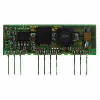
Page 3
... GS-R12FP 1 Pin settings 1.1 Pin connection and mechanical data (dimensions in mm) Figure 1. Pin connection GS-R12FVxxx1.9 Figure 2. Pin connection GS-R12FSxxx1.9 Pin settings 3/14 ...
Page 4
... Pin settings 1.2 Pin description Table 2. Pin description Name Input/output 6 Input/output 4/14 Function A logic high level disables the device. When the pin is open, an INH internal pull up disables the device Sync Master/slave synchronization V 3.3 V reference voltage ref Input + DC input voltage Input + DC input voltage ...
Page 5
... GS-R12FP 2 Maximum ratings 2.1 Absolute maximum ratings Table 3. Absolute maximum ratings Symbol V DC input voltage I I Maximum output current out V INH 1 V Sync 2.2 Thermal data Table 4. Thermal data Symbol T Storage temperature range STG T Operating ambient temperature OP 2.3 Thermal de-rating Table 5. ...
Page 6
... ÷ 4 ÷ 4 > 2.2 V inh 1 4.5 ÷ ÷ ref Device ON Device OFF = 4.5 ÷ GS-R12FP Min Typ Max 1.9 A TBD o 0 1.9 2.3 2.7 50 100 500 3.2 3.3 3.399 0.8 2 ÷ 1.22 1.235 1.25 O Unit mVpp mV/° µA kHz V mA ...
Page 7
... GS-R12FP 4 Application information 4.1 Input voltage The recommended maximum operating DC input voltage including ripple voltage. 4.2 Reference voltage No capacitor is required for stability. 4.3 Inhibit function The inhibit feature allows to put the device in stand-by mode. With INH pin 1 is higher than 2.2 V the device is disabled and the current consumption is reduced to less than 100 µ ...
Page 8
... An hysteresis of approximately 20 °C avoids that the devices turns ON and OFF continuously. 4.7 Output voltage programming (GS-R12FP0001.9 only) The GS-R12FP0001.9 output voltage is 5.54 V ± reduce this value connect a resistor between pin 10 (FB) and pin 9 (V The resistor must be located very close to the proper pins, to minimize the injected noise (see Figure 4) ...
Page 9
... GS-R12FP 4.9 Soldering Soldering phase has to be execute with care : in order to avoid undesired melting phenomenon, particular attention has to be take on the set up of the peak temperature. Here following some suggestions for the temperature profile based on IPC/JEDEC J-STD-020C ,July 2004 recommendations. Table 7. ...
Page 10
... It turns off the power stage when the OVP threshold is reached. This threshold is typically 30 % higher than the feedback voltage. Figure 4. Output voltage programming 4, 5 Vin GS-RxxFp000z.z Figure 6. Multiple units synchronization 4, 5 Vin GS-RxxFpyyyz.z 10/14 Figure Rload Rload 8, 9 Vin 6, 7 GS-R12FP Loop compensation Vin GS-RxxFp000z Rload 8, 9 GS-RxxFpyyyz Rload ...
Page 11
... GS-R12FP Figure 7. PCB footprint for GS-R12FSxxx1.9 (dimensions in mm) Additional features and protections 11/14 ...
Page 12
... Ordering scheme 6 Ordering scheme Table 8. Ordering information scheme Input voltage Package V = Vertical S = SMD Output voltage 018 = 1.8 V 025 = 2.5 V 033 = 3.3 V 050 = 5.0 V ÷ 000 = 1.235 5.5 V Output current 1.9 = 1.9 A 12/14 GS- R12 FV GS-R12FP 018 1.9 ...
Page 13
... GS-R12FP 7 Revision history Table 9. Document revision history Date 13-Oct-2006 27-Feb-2008 Revision 1 Initial release 2 Added: Section 4.9: Soldering on page 9 Revision history Changes 13/14 ...
Page 14
... Australia - Belgium - Brazil - Canada - China - Czech Republic - Finland - France - Germany - Hong Kong - India - Israel - Italy - Japan - Malaysia - Malta - Morocco - Singapore - Spain - Sweden - Switzerland - United Kingdom - United States of America 14/14 Please Read Carefully: © 2008 STMicroelectronics - All rights reserved STMicroelectronics group of companies www.st.com GS-R12FP ...