LTM4611IV#PBF Linear Technology, LTM4611IV#PBF Datasheet - Page 4
LTM4611IV#PBF
Manufacturer Part Number
LTM4611IV#PBF
Description
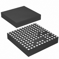
IC UMODULE DC/DC LV 15A 133-LGA
Manufacturer
Linear Technology
Series
µModuler
Type
Point of Load (POL) Non-Isolatedr
Datasheet
1.LTM4611EVPBF.pdf
(28 pages)
Specifications of LTM4611IV#PBF
Output
0.8 ~ 5 V
Number Of Outputs
1
Power (watts)
75W
Mounting Type
Surface Mount
Voltage - Input
1.5 ~ 5.5 V
Package / Case
133-LGA
1st Output
0.8 ~ 5 VDC @ 15A
Size / Dimension
0.59" L x 0.59" W x 0.17" H (15mm x 15mm x 4.32mm)
Power (watts) - Rated
75W
Operating Temperature
-40°C ~ 125°C
Efficiency
94%
Lead Free Status / RoHS Status
Lead free / RoHS Compliant
3rd Output
-
2nd Output
-
Available stocks
Company
Part Number
Manufacturer
Quantity
Price


elecTrical characTerisTics
LTM4611
junction temperature range, otherwise specifications are at T
SYMBOL
Control Section
V
I
V
I
t
R
V
V
DIFFV
V
A
V
SR
GBP
CMRR
R
INTV
V
V
Oscillator and Phase-Locked Loop
f
f
FB
TRACK/SS
ON(MIN)
S
SYNC
INTVCC
INTVCC
FB
OVL
FBHI
OSNS
OSNS – CM RANGE
OS
PGOOD
IN
V
CC
OUT
+
,
Linear Regulator
Load Reg
Range
PARAMETER
Voltage at V
Feedback Overvoltage Lockout
Track Pin Soft-Start Pull-Up
Current
Minimum On-Time
Resistor Between V
and V
Common Mode Input Range
DIFF_AMP Output Voltage Range
DIFF_AMP Input Offset Voltage
Magnitude
DIFF_AMP Differential Gain
PGOOD Trip Level
DIFF_AMP Slew Rate
DIFF_AMP Gain-Bandwidth
Product
DIFF_AMP Common Mode
Rejection
DIFF_AMP Input Resistance
Internal V
INTV
Output Ripple Voltage Frequency
SYNC Capture Range
CC
FB
Load Regulation
Pins
CC
FB
Voltage
Pin
OUT_LCL
CONDITIONS
I
TRACK/SS = 0V
(Note 5)
V
V
V
V
1.5V < V
I
V
0.85V ≤ PLLFLTR/f
OUT
CC
IN
IN
FB
OSNS
IN
V
V
V
V
FB
FB
FB
FB
= 0 to 50mA
= 3.3V, V
= 3.3V, Run > 1.5V
= 3.3V, DIFFV
with Respect to Set Output
= 0A, V
Ramping Positive, PGOOD Transitioning
Ramping Positive, PGOOD Transitioning
Ramping Negative, PGOOD Transitioning
Ramping Negative, PGOOD Transitioning
+ to GND
IN
The
< 5.5V
A
OUT
OUT
= 25°C, V
l
= V
denotes the specifications which apply over the full internal operating
= 1.5V,
OUT
SET
FB
Load = 100k
≤ 2.0V
IN
= 3.3V, per the typical application in Figure 21.
l
l
l
0.783
60.05
0.84
19.9
MIN
–10
–10
280
360
0.9
4.8
0
0
5
5
0.797
60.40
TYP
0.87
–7.5
–7.5
20.0
–10
100
1.4
0.5
7.5
7.5
90
1
2
3
5
INTV
INTV
0.811
60.75
MAX
0.89
1.25
20.1
835
710
1.9
5.2
–5
10
10
–5
CC
2
CC
– 1
UNITS
V/µs
MHz
4611f
V/V
kHz
kHz
mV
mV
kΩ
kΩ
nA
µA
dB
ns
%
%
%
%
%
V
V
V
V
V
Related parts for LTM4611IV#PBF
Image
Part Number
Description
Manufacturer
Datasheet
Request
R

Part Number:
Description:
Ltm4611 Ultralow Vin, 15a Dc/dc ?module Regulator Features
Manufacturer:
Linear Technology Corporation
Datasheet:

Part Number:
Description:
CD ROM LINEARVIEW DATASHEETS
Manufacturer:
Linear Technology
Part Number:
Description:
Standalone Linear Li-Ion Battery Charger with Thermal Regulation in ThinSOT
Manufacturer:
Linear Technology Corporation
Datasheet:
Part Number:
Description:
Low noise, high frequency, 8th order linear phase lowpass filter
Manufacturer:
Linear Technology Corporation
Datasheet:
Part Number:
Description:
Manufacturer:
Linear Technology Corporation
Datasheet:
Part Number:
Description:
Manufacturer:
Linear Technology Corporation
Datasheet:
Part Number:
Description:
Manufacturer:
Linear Technology Corporation
Datasheet:
Part Number:
Description:
Manufacturer:
Linear Technology Corporation
Datasheet:
Part Number:
Description:
Manufacturer:
Linear Technology Corporation
Datasheet:
Part Number:
Description:
Manufacturer:
Linear Technology Corporation
Datasheet:
Part Number:
Description:
Manufacturer:
Linear Technology Corporation
Datasheet:
Part Number:
Description:
Dual and Quad, JFET Input Precision High Speed Op Amps
Manufacturer:
Linear Technology Corporation
Datasheet:
Part Number:
Description:
Manufacturer:
Linear Technology Corporation
Datasheet:
Part Number:
Description:
1, 2, 6 and 8 Channel, 10-Bit Serial I/O Data Acquisition Systems
Manufacturer:
Linear Technology Corporation
Datasheet:
Part Number:
Description:
Manufacturer:
Linear Technology Corporation
Datasheet: