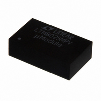
LTM8025MPV#PBF Linear Technology, LTM8025MPV#PBF Datasheet - Page 15

LTM8025MPV#PBF
Manufacturer Part Number
LTM8025MPV#PBF
Description
IC CONVERTER BUCK 3A ADJ 70LGA
Manufacturer
Linear Technology
Series
µModuler
Type
Point of Load (POL) Non-Isolatedr
Datasheet
1.LTM8025EVPBF.pdf
(20 pages)
Specifications of LTM8025MPV#PBF
Design Resources
LTM8025 Spice Model
Output
0.8 ~ 24 V
Number Of Outputs
1
Power (watts)
72W
Mounting Type
Surface Mount
Voltage - Input
3.6 ~ 36 V
Package / Case
70-LGA
1st Output
0.8 ~ 24 VDC @ 3A
Size / Dimension
0.59" L x 0.35" W x 0.17" H (15mm x 9mm x 4.32mm)
Power (watts) - Rated
72W
Operating Temperature
-55°C ~ 125°C
Lead Free Status / RoHS Status
Lead free / RoHS Compliant
3rd Output
-
2nd Output
-
Available stocks
Company
Part Number
Manufacturer
Quantity
Price
APPLICATIONS INFORMATION
Thermal Considerations
The LTM8025 output current may need to be derated if it is
required to operate in a high ambient temperature or deliver
a large amount of continuous power. The amount of current
derating is dependent upon the input voltage, output power
and ambient temperature. The temperature rise curves
given in the Typical Performance Characteristics section
can be used as a guide. These curves were generated by a
LTM8025 mounted to a 58cm
board. Boards of other sizes and layer count can exhibit
different thermal behavior, so it is incumbent upon the user
to verify proper operation over the intended system’s line,
load and environmental operating conditions.
The junction to air and junction to board thermal resis-
tances given in the Pin Confi guration diagram may also
be used to estimate the LTM8025 internal temperature.
These thermal coeffi cients are determined for maximum
output power per JESD 51-9 “JEDEC Standard, Test Boards
for Area Array Surface Mount Package Thermal Measure-
ments” through analysis and physical correlation. Bear in
mind that the actual thermal resistance of the LTM8025
to the printed circuit board depends upon the design of
the circuit board.
TYPICAL APPLICATIONS
3.6V TO 24V
V
IN
10μF
147k
1.8V Step-Down Converter
V
RUN/SS
BIAS
SHARE
RT
IN
SYNC
LTM8025
2
4-layer FR4 printed circuit
GND
PGOOD
V
AUX
ADJ
OUT
383k
300μF
V
1.8V AT 3A
OUT
8025 TA02
The die temperature of the LTM8025 must be lower than
the maximum rating of 125°C, so care should be taken in
the layout of the circuit to ensure good heat sinking of the
LTM8025. The bulk of the heat fl ow out of the LTM8025
is through the bottom of the module and the LGA pads
into the printed circuit board. Consequently a poor printed
circuit board design can cause excessive heating, result-
ing in impaired performance or reliability. Please refer to
the PCB Layout section for printed circuit board design
suggestions.
The LTM8025 is equipped with a thermal shutdown that
will inhibit power switching at high junction temperatures.
The activation threshold of this function, however, is above
125°C to avoid interfering with normal operation. Thus,
it follows that prolonged or repetitive operation under a
condition in which the thermal shutdown activates neces-
sarily means that the internal components are subjected
to temperatures above the 125°C rating for prolonged
or repetitive intervals, which may damage or impair the
reliability of the device.
Finally, be aware that at high ambient temperatures the
internal Schottky diode will have signifi cant leakage current
increasing the quiescent current of the LTM8025.
4.1V TO 36V
V
IN
*
*RUNNING VOLTAGE RANGE. PLEASE REFER TO
APPLICATIONS INFORMATION SECTION FOR START-UP DETAILS
4.7μF
137k
2.5V Step-Down Converter
3.3V
V
RUN/SS
BIAS
SHARE
RT
IN
SYNC
LTM8025
GND
PGOOD
V
AUX
ADJ
OUT
LTM8025
226k
200μF
15
V
2.5V AT 3A
OUT
8025fa
8025 TA03


