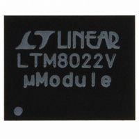
LTM8022EV#PBF Linear Technology, LTM8022EV#PBF Datasheet - Page 12

LTM8022EV#PBF
Manufacturer Part Number
LTM8022EV#PBF
Description
IC DC/DC UMODULE 1A 50-LGA
Manufacturer
Linear Technology
Series
µModuler
Type
Point of Load (POL) Non-Isolatedr
Datasheet
1.LTM8022EVPBF.pdf
(20 pages)
Specifications of LTM8022EV#PBF
Design Resources
LTM8022 Spice Model
Output
0.8 ~ 10 V
Number Of Outputs
1
Power (watts)
10W
Mounting Type
Surface Mount
Voltage - Input
3.6 ~ 36 V
Package / Case
50-LGA
1st Output
0.8 ~ 10 VDC @ 1A
Size / Dimension
0.44" L x 0.35" W x 0.11" H (11.25mm x 9mm x 2.82mm)
Power (watts) - Rated
10W
Operating Temperature
-40°C ~ 85°C
Lead Free Status / RoHS Status
Lead free / RoHS Compliant
3rd Output
-
2nd Output
-
Available stocks
Company
Part Number
Manufacturer
Quantity
Price
APPLICATIONS INFORMATION
PCB Layout
Most of the headaches associated with PCB layout have
been alleviated or even eliminated by the high level of
integration of the LTM8022. The LTM8022 is nevertheless
a switching power supply, and care must be taken to
minimize EMI and ensure proper operation. Even with the
high level of integration, you may fail to achieve specifi ed
operation with a haphazard or poor layout. See Figure 4
for a suggested layout.
Ensure that the grounding and heatsinking are acceptable.
A few rules to keep in mind are:
1. Place the R
2. Place the C
LTM8022
12
tive pins as possible.
and GND connection of the LTM8022.
ADJ
IN
capacitor as close as possible to the V
and R
T
resistors as close to their respec-
GND PLANE
Figure 4. Layout Showing Suggested External
Components, GND Plane and Thermal Vias
V
OUT
PLANE
C
OUT
IN
3. Place the C
4. Place the C
5. Connect all of the GND connections to as large a copper
6. Use vias to connect the GND copper area to the boards
SHARE
AUX
V
ground current fl ow directly adjacent or underneath the
LTM8022.
pour or plane area as possible on the top layer. Avoid
breaking the ground connection between the external
components and the LTM8022.
internal ground plane. Liberally distribute these GND vias
to provide both a good ground connection and thermal
path to the internal planes of the printed circuit board.
C
R
IN
T
OUT
BIAS
LTM8022
and GND connection of the LTM8022.
V
IN
PLANE
R
ADJ
OUT
IN
SYNC
PG
RUN/SS
and C
capacitor as close as possible to the
OUT
capacitors such that their
8022fd


