AFBR-5905Z Avago Technologies US Inc., AFBR-5905Z Datasheet - Page 6
AFBR-5905Z
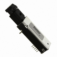
Manufacturer Part Number
AFBR-5905Z
Description
TXRX OPT OC3 MTRJ SFF 2X5DIP
Manufacturer
Avago Technologies US Inc.
Datasheet
1.AFBR-5905Z.pdf
(13 pages)
Specifications of AFBR-5905Z
Applications
General Purpose
Wavelength
1300nm
Voltage - Supply
3.3V
Connector Type
MTRJ
Mounting Type
Through Hole
Data Rate Max
0.1Gbps
Supply Voltage
3.3V
Wavelength Typ
1308nm
Leaded Process Compatible
Yes
Lead Free Status / RoHS Status
Lead free / RoHS Compliant
Data Rate
-
Lead Free Status / RoHS Status
Lead free / RoHS Compliant, Lead free / RoHS Compliant
Other names
516-1994


Transceiver Signaling Operating Rate Range and BER
Performance
For purposes of definition, the symbol (Baud) rate, also
called signaling rate, is the reciprocal of the symbol time.
Data rate (bits/sec) is the symbol rate divided by the en-
coding factor used to encode the data (symbols/bit).
When used in 155 Mb/s SONET OC-3 applications the
performance of the 1300 nm transceivers, AFBR-5905 is
guaranteed to the full conditions listed in product speci-
fication tables. The transceivers may be used for other ap-
plications at signaling rates different than 155 Mb/s with
some variation in the link optical power budget. Figure
5 gives an indication of the typical performance of these
products at different rates.
These transceivers can also be used for applications which
require different Bit Error Rate (BER) performance. Figure
6 illustrates the typical trade-off between link BER and the
receivers input optical power level.
Transceiver Jitter Performance
The Avago 1300 nm transceivers are designed to oper-
ate per the system jitter allocations stated in Table B1 of
Annex B of the draft ANSI T1E1.2 Revision 3 standard. The
Avago 1300 nm transmitters will tolerate the worst case
input electrical jitter allowed in Annex B without violat-
ing the worst case output optical jitter requirements.
The Avago 1300 nm receivers will tolerate the worst case
input optical jitter allowed in Annex B without violating
the worst case output electrical jitter allowed. The jitter
specifications stated in the following 1300 nm transceiver
6
Transceiver Signaling Operating
Rate Range and BER Performance
For purposes of definition, the
symbol (Baud) rate, also called
signaling rate, is the reciprocal
of the symbol time. Data rate
(bits/sec) is the symbol rate
divided by the encoding factor
used to encode the data
(symbols/bit).
When used in 155 Mb/s
SONET OC-3 applications the
performance of the 1300 nm
transceivers, AFBR-5905 is
guaranteed to the full
conditions listed in product
specification tables.
The transceivers may be used
for other applications at
signaling rates different than
155 Mb/s with some variation
in the link optical power
budget. Figure 5 gives an
indication of the typical
performance of these products
at different rates.
Figure 5. Transceiver Relative Optical Power
Budget at Constant BER vs. Signaling Rate.
These transceivers can also be
used for applications which
require different Bit Error Rate
(BER) performance. Figure 6
illustrates the typical trade-off
between link BER and the
receivers input optical power
-0.5
2.5
1.5
0.5
-1
2
1
0
0
CONDITIONS:
1. PRBS 2
2. DATA SAMPLED AT CENTER OF DATA SYMBOL.
3. BER = 10
4. T
5. V
6. INPUT OPTICAL RISE/FALL TIMES = 1.0/2.1 ns.
A
CC
= +25 C
25
= 3.3 V dc
7
-1
-6
50
SIGNAL RATE (MBd)
75
100
Transceiver Signaling Operating
Rate Range and BER Performance
For purposes of definition, the
symbol (Baud) rate, also called
signaling rate, is the reciprocal
of the symbol time. Data rate
(bits/sec) is the symbol rate
divided by the encoding factor
used to encode the data
(symbols/bit).
When used in 155 Mb/s
SONET OC-3 applications the
performance of the 1300 nm
transceivers, AFBR-5905 is
guaranteed to the full
conditions listed in product
specification tables.
The transceivers may be used
for other applications at
signaling rates different than
155 Mb/s with some variation
in the link optical power
budget. Figure 5 gives an
indication of the typical
performance of these products
at different rates.
125
150
175
200
Figure 6. Bit Error Rate vs. Relative Receiver
Input Optical Power.
Transceiver Jitter Performance
The Agilent 1300 nm
transceivers are designed to
operate per the system jitter
allocations stated in Table B1
of Annex B of the draft ANSI
T1E1.2 Revision 3 standard.
The Agilent 1300 nm
transmitters will tolerate the
worst case input electrical
jitter allowed in Annex B
without violating the worst
case output optical jitter
requirements.
The Agilent 1300 nm receivers
will tolerate the worst case
input optical jitter allowed in
Annex B without violating the
worst case output electrical
jitter allowed.
The jitter specifications stated
in the following 1300 nm
transceiver specification tables
are derived from the values in
Table B1 of Annex B. They
represent the worst case jitter
contribution that the
transceivers are allowed to
make to the overall system
jitter without violating the
Annex B allocation example. In
practice, the typical
contribution of the Agilent
transceivers is well below
1 x 10⁻¹⁰
1 x 10-11
1 x 10-12
1 x 10⁻²
1 x 10⁻³
1 x 10⁻⁴
1 x 10⁻⁵
1 x 10⁻⁶
1 x 10⁻⁷
1 x 10⁻⁸
1 x 10⁻⁹
-6
CONDITIONS:
1. 125 MBd
2. PRBS 2
3. CENTER OF SYMBOL SAMPLING
4. T
5. V
6. INPUT OPTICAL RISE/FALL TIMES = 1.0/2.1 ns.
RELATIVE INPUT OPTICAL POWER - dB
A
CC
= +25C
= 3.3 V dc
-4
7
-1
-2
HFBR-5905 SERIES
specification tables are derived from the values in Table
B1 of Annex B. They represent the worst case jitter con-
tribution that the transceivers are allowed to make to the
overall system jitter without violating the Annex B alloca-
tion example. In practice, the typical contribution of the
Avago transceivers is well below these maximum allowed
amounts.
Recommended Handling Precautions
Avago recommends that normal static precautions be
taken in the handling and assembly of these transceiv-
ers to prevent damage which may be induced by electro-
static discharge (ESD). The AFBR-5905Z series of transceiv-
ers meet MIL-STD- 883C Method 3015.4 Class 2 products.
Care should be used to avoid shorting the receiver data or
signal detect outputs directly to ground without proper
current limiting impedance.
Solder and Wash Process Compatibility
The transceivers are delivered with protective process
plugs inserted into the MT-RJ receptacle. This process
plug protects the optical subassemblies during wave sol-
der and aqueous wash processing and acts as a dust cover
during shipping. These transceivers are compatible with
either industry standard wave or hand solder processes.
Shipping Container
The transceiver is packaged in a shipping container de-
signed to protect it from mechanical and ESD damage
during shipment or storage.
Figure 6. Bit Error Rate vs. Relative Receiver
Input Optical Power.
Transceiver Jitter Performance
The Agilent 1300 nm
transceivers are designed to
operate per the system jitter
allocations stated in Table B1
of Annex B of the draft ANSI
T1E1.2 Revision 3 standard.
CENTER OF SYMBOL
1 x 10⁻¹⁰
1 x 10-11
1 x 10-12
0
1 x 10⁻²
1 x 10⁻³
1 x 10⁻⁴
1 x 10⁻⁵
1 x 10⁻⁶
1 x 10⁻⁷
1 x 10⁻⁸
1 x 10⁻⁹
-6
CONDITIONS:
1. 125 MBd
2. PRBS 2
3. CENTER OF SYMBOL SAMPLING
4. T
5. V
6. INPUT OPTICAL RISE/FALL TIMES = 1.0/2.1 ns.
2
RELATIVE INPUT OPTICAL POWER - dB
A
CC
= +25C
= 3.3 V dc
-4
7
-1
4
Recommended Handling Precautions
Agilent recommends that
normal static precautions be
taken in the handling and
assembly of these transceivers
to prevent damage which may
be induced by electrostatic
discharge (ESD).
The AFBR-5905Z series of
transceivers meet MIL-STD-
883C Method 3015.4 Class 2
products.
Care should be used to avoid
shorting the receiver data or
signal detect outputs directly
to ground without proper
current limiting impedance.
Solder and Wash Process
Compatibility
The transceivers are delivered
with protective process plugs
inserted into the MT-RJ
receptacle. This process plug
protects the optical
subassemblies during wave
solder and aqueous wash
processing and acts as a dust
cover during shipping.
These transceivers are compat-
ible with either industry
standard wave or hand solder
processes.
Shipping Container
The transceiver is packaged in
a shipping container designed
to protect it from mechanical
and ESD damage during
shipment or storage.
-2
HFBR-5905 SERIES
CENTER OF SYMBOL
0
2
4
Recommended Handling Precau
Agilent recommends that
normal static precautions b
taken in the handling and
assembly of these transceiv
to prevent damage which m
be induced by electrostatic
discharge (ESD).
The AFBR-5905Z series of
transceivers meet MIL-STD
883C Method 3015.4 Class
products.
Care should be used to avo
shorting the receiver data o
signal detect outputs direct
to ground without proper
current limiting impedance.
Solder and Wash Process
Compatibility
The transceivers are deliver
with protective process plu
inserted into the MT-RJ
receptacle. This process plu
protects the optical
subassemblies during wave
Related parts for AFBR-5905Z
Image
Part Number
Description
Manufacturer
Datasheet
Request
R

Part Number:
Description:
650nm FE Transceiver Eval Kit
Manufacturer:
Avago Technologies US Inc.
Datasheet:

Part Number:
Description:
TXRX ETHERNET 125MBD MMF 2X5
Manufacturer:
Avago Technologies US Inc.
Datasheet:

Part Number:
Description:
TXRX OPT SFP DGTL 850NM IND
Manufacturer:
Avago Technologies US Inc.
Datasheet:

Part Number:
Description:
TXRX OPT SFF 4/2/1GBD 2X7
Manufacturer:
Avago Technologies US Inc.
Datasheet:

Part Number:
Description:
TXRX OPT SFP 4/2/1GBD 850NM
Manufacturer:
Avago Technologies US Inc.
Datasheet:

Part Number:
Description:
TXRX OPT XFP 10GB/S 850NM
Manufacturer:
Avago Technologies US Inc.
Datasheet:

Part Number:
Description:
TXRX OPT 1X9 100MBPS ST EXT TEMP
Manufacturer:
Avago Technologies US Inc.
Datasheet:

Part Number:
Description:
TXRX OPT 1X9 100MBPS SC EXT TEMP
Manufacturer:
Avago Technologies US Inc.
Datasheet:

Part Number:
Description:
TXRX OPT 1X9 100MBPS DUPLEX SC
Manufacturer:
Avago Technologies US Inc.
Datasheet:

Part Number:
Description:
TXRX OPT 1X9 100MBPS DUPLEX ST
Manufacturer:
Avago Technologies US Inc.
Datasheet:

Part Number:
Description:
OPTOCOUPLER GATE DRV 2A 16-SOIC
Manufacturer:
Avago Technologies US Inc.
Datasheet:
Part Number:
Description:
OPTOCOUPLER 2CH 2.5A 16-SOIC
Manufacturer:
Avago Technologies US Inc.
Datasheet:

Part Number:
Description:
OPTOCOUPLER GATE DRV 0.4A 16SOIC
Manufacturer:
Avago Technologies US Inc.
Datasheet:

Part Number:
Description:
OPTOCOUPLER 2.0A 250KHZ 8-DIP
Manufacturer:
Avago Technologies US Inc.
Datasheet:

Part Number:
Description:
OPTOCOUPLER 2.0A 250KHZ GW 8-SMD
Manufacturer:
Avago Technologies US Inc.
Datasheet: