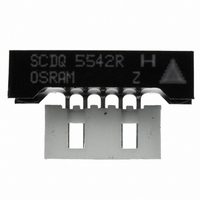
SCDQ5542R OSRAM Opto Semiconductors Inc, SCDQ5542R Datasheet - Page 8

SCDQ5542R
Manufacturer Part Number
SCDQ5542R
Description
INTELLIGENT DISP 4CHAR 5X5 HER
Manufacturer
OSRAM Opto Semiconductors Inc
Series
Intelligent Display®r
Datasheet
1.SCDQ5542P.pdf
(16 pages)
Specifications of SCDQ5542R
Millicandela Rating
5.4mcd
Size / Dimension
0.78" L x 0.40" W x 0.20" H (19.91mm x 10.16mm x 5.08mm)
Color
Red
Configuration
5 x 5
Number Of Digits
4
Character Size
0.134 in
Illumination Color
Super Red
Wavelength
630 nm
Maximum Operating Temperature
+ 85 C
Minimum Operating Temperature
- 40 C
Luminous Intensity
5.4 mcd
Viewing Area (w X H)
3.4 mm x 3.4 mm
Display Type
5 x 7 Dot Matrix
Lead Free Status / RoHS Status
Lead free / RoHS Compliant
Voltage - Forward (vf) Typ
-
Internal Connection
-
Lead Free Status / Rohs Status
Details
Other names
475-1426
Q68100A1078R
SCDQ5542R
Q68100A1078R
SCDQ5542R
Available stocks
Company
Part Number
Manufacturer
Quantity
Price
Company:
Part Number:
SCDQ5542R
Manufacturer:
OSRAM Opto Semiconductors Inc
Quantity:
135
SCDQ Block Diagram
The following explains how to format the serial data to be loaded into the display. The user supplies a string of bit mapped decoded char-
acters. The contents of this string is shown in Figure „Loading Serial Character Data A“ (page 8). Figure „Loading Serial Character
Data B“ (page 8) shows that each character consists of six 8 bit words. The first word encodes the display character location and the suc-
ceeding five bytes are row data. The row data represents the status (On, Off) of individual column LEDs. Figure „Loading Serial Character
Data C“ (page 8) shows that each 8 bit word is formatted to include a three bit Operational Code (OPCODE) defined by bits D7–D5 and
five bits (D4–D0) representing Column Data, Character Address, or Control Word Data.
Figure „Loading Serial Character Data D“ (page 8) shows the sequence for loading the bytes of data. Bringing the LOAD line low enables
the serial register to accept data. The shift action occurs on the low to high transition of the serial data clock (SDCLK). The least significant
bit (D0) is loaded first. After eight clock pulses the LOAD line is brought high. With this transition the OPCODE is decoded. The decoded
OPCODE directs D4–D0 to be latched in the Character Address register, stored in the RAM as Column data, or latched in the Control
Word register. The control IC requires a minimum 600 ns delay between successive byte loads.
Loading Serial Character Data
2006-05-12
SCDQ5541P/Q/R, SCDQ5542P/Q/R, SCDQ5543P/Q/R, SCDQ5544P/Q/R
SDCLK
SDATA
LOAD
A
B
C
D
LOAD
SDCLK
DATA
D0
0
Character 0
Character
Character
Address 0
D1
0
B
D2
&
0
Address
D0
C
D3
0
Column Data
Character 1
D4
Row 0
0
D1
D
D5
5
3
1
Opcode
D2
D6
0
Column Data
Character 2
D7
D3
1
Row 1
Counter Chain
600 ns
TBL
min.
Oscillator
D4
& Timing
8
D0
C4
D5
Column Data
Character 3
Row 2
Column Data
C3
D1
3
D6
D2
C2
D7
D3
C1
Row Decoder
Column Data
Power Down
Lamp Test
Brightness
& Driver
D4
C0
Row 3
Display Multiplexer
Dual Port Ram
D5
0
Opcode
20 x 5 bit
TBL
D6
0
5
Column Data
D7
0
Row 4
Column Logic
Characters
600 ns
IDTC5043
4 - 5 x 5
& Driver
TBL
min.
DD
IDBD5061
20
20


